DAC-HP16BMM中文资料
16-Bit, High-Performance
Digital-to-Analog Converters
INN O VAT IO N a n d E X C
E L L E N C E
FEATURES
?16-Bit resolution
?3 Output voltage ranges
?±15ppm/°C maximum gain tempco
?Integral nonlinearity error ±0.003%FSR, max.?14 Bits monotonic from +10°C to +40°C
?
High-reliability MIL-STD–883 models available
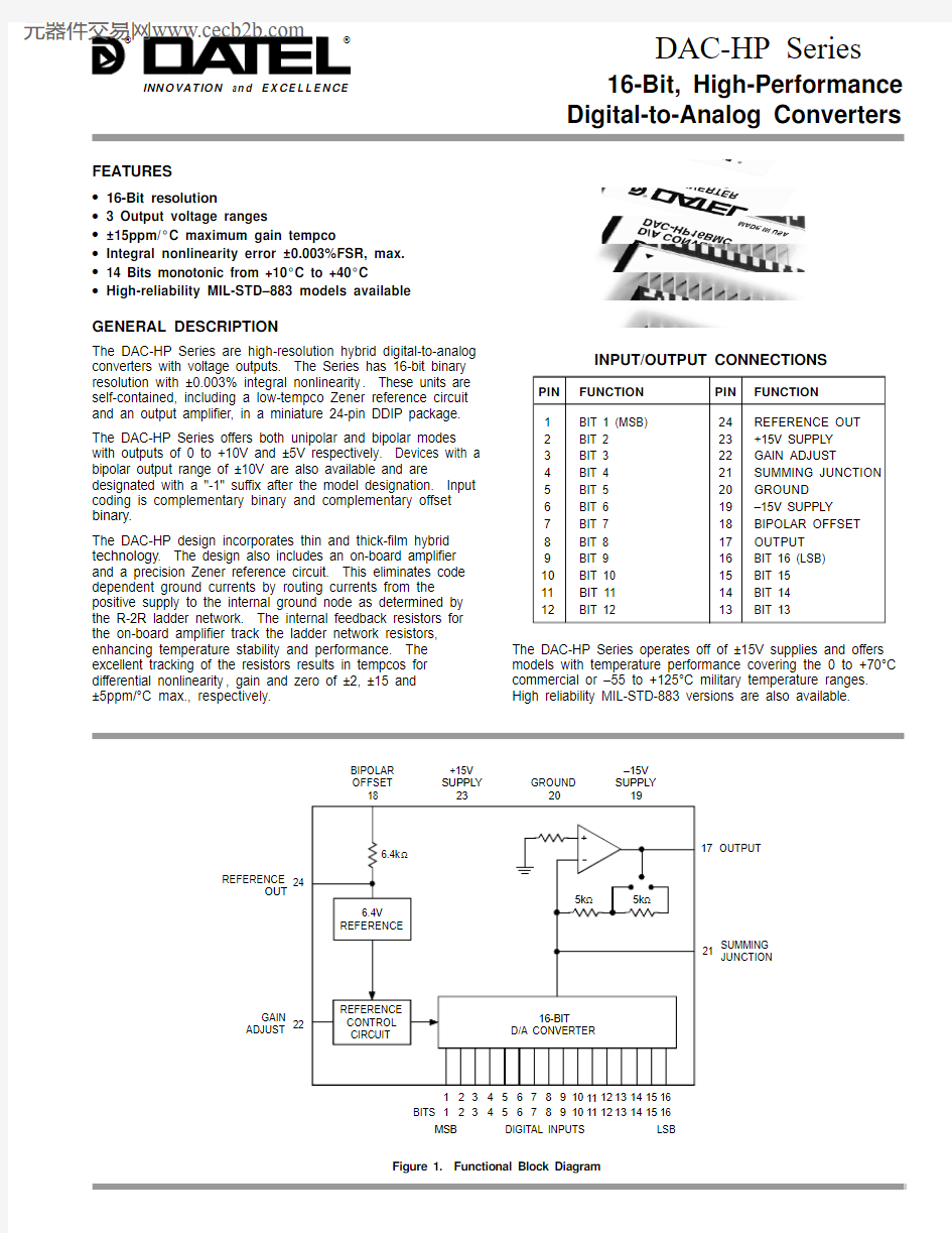
Figure 1. Functional Block Diagram
MSB
BITS
LSB
1234REFERENCE OUT
24
GAIN
ADJUST
23
BIPOLAR
OFFSET 18+15V SUPPLY 22
20
19
1721
SUMMING JUNCTION
567891011
12DIGITAL INPUTS
GROUND
OUTPUT
–15V SUPPLY 13141516
12345678910111213141516GENERAL DESCRIPTION
The DAC-HP Series are high-resolution hybrid digital-to-analog converters with voltage outputs. The Series has 16-bit binary resolution with ±0.003% integral nonlinearity . These units are self-contained, including a low-tempco Zener reference circuit and an output amplifier, in a miniature 24-pin DDIP package.The DAC-HP Series offers both unipolar and bipolar modes with outputs of 0 to +10V and ±5V respectively . Devices with a bipolar output range of ±10V are also available and are
designated with a "-1" suffix after the model designation. Input coding is complementary binary and complementary offset binary.
The DAC-HP design incorporates thin and thick-film hybrid technology . The design also includes an on-board amplifier and a precision Zener reference circuit. This eliminates code dependent ground currents by routing currents from the
positive supply to the internal ground node as determined by the R-2R ladder network. The internal feedback resistors for the on-board amplifier track the ladder network resistors,enhancing temperature stability and performance. The excellent tracking of the resistors results in tempcos for differential nonlinearity , gain and zero of ±2, ±15 and ±5ppm/°C max., respectively.
The DAC-HP Series operates off of ±15V supplies and offers models with temperature performance covering the 0 to +70°C commercial or –55 to +125°C military temperature ranges.High reliability MIL-STD-883 versions are also available.
INPUT/OUTPUT CONNECTIONS
DATEL, Inc., 11 Cabot Boulevard, Mansfield, MA 02048-1194 (U.S.A.) Tel: 508-339-3000 Fax: 508-339-6356 ? For immediate assistance 800-233-2765
TECHNICAL NOTES
1.It is recommended that these converters be operated with local supply bypass capacitors of 1μF (tantalum type) at the +15V and –15V supply pins. The capacitors should be connected as close to the pins as possible. In high-frequency noise environments, an additional 0.01μF ceramic capacitor should be used in parallel with each tantalum bypass.
2.When laying out the circuit board for this device, isolate the analog, digital and power grounds as much as possible from each other before joining them at pin 20.
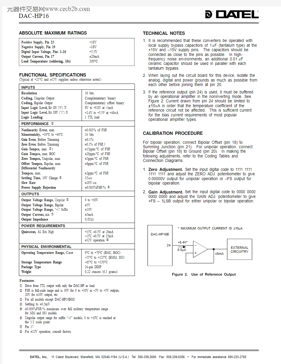
3.If the reference output (pin 24) is used, it must be buffered by an operational amplifier in the noninverting mode. See Figure 2. Current drawn from pin 24 should be limited to ±10μA in order that the temperature coefficient of the reference circuit not be affected. This is sufficient current for the bias current requirements of most popular operational amplifier types.
ABSOLUTE MAXIMUM RATINGS
Positive Supply, Pin 23+18V Negative Supply, Pin 19
–18V Digital Input Voltage, Pins 1–16+5.5V Output Current, Pin 17
±20mA Lead Temperature (soldering, 10s)
300°C
FUNCTIONAL SPECIFICATIONS
(Typical at +25°C and ±15V supplies unless otherwise noted.)Footnotes
Drive from TTL output with only the DAC-HP as load.
FSR is full-scale range and is 10V for 0 to +10V or –5V to +5V outputs,
20V for ±10V output, etc
For all models except DAC-HP16BGC Settling to ±0.5mV
±0.006%FSR/% maximum over full military temperature range
for MM and 883 models.
Unipolar output range for suffix “–1” models, 0 to +10V, is reached at
the 1/2 scale point. Pin 17.
For ±12V operation, consult factory.
CALIBRATION PROCEDURE
For bipolar operation, connect Bipolar Offset (pin 18) to
Summing Junction (pin 21). For unipolar operation, connect Bipolar Offset (pin 18) to Ground (pin 20). In making the following adjustments, refer to the Coding Tables and Connection Diagrams.
1.Zero Adjustment. Set the input digital code to 1111 11111111 1111 and adjust the ZERO ADJ. potentiometer to give 0.00000V output for unipolar operation or –FS output for bipolar operation.
2.Gain Adjustment. Set the input digital code to 0000 00000000 0000 and adjust the GAIN ADJ. potentiometer to give +FS – 1LSB output for either unipolar or bipolar operation.
Figure 2. Use of Reference Output
CODING TABLES
Table 1. Bipolar Output — Complementary Offset Binary
Table 2. Unipolar Output — Complementary Binary
CONNECTION DIAGRAMS
Figure 4. Bipolar Operations
Figure 3. Unipolar Operations
REFERENCE OUT
24BIPOLAR OFFSET 18201721SUMMING JUNCTION
GROUND
OUTPUT
I Figure 5. Output Circuit
+15V
–15V
+15V
–15V
MECHANICAL DIMENSIONS Inches (mm)
ORDERING INFORMATION
DATEL, Inc. 11 Cabot Boulevard, Mansfield, MA 02048-1151 Tel: (508) 339-3000 (800) 233-2765 Fax: (508) 339-6356 Internet: https://www.sodocs.net/doc/9516257517.html, Email: sales@https://www.sodocs.net/doc/9516257517.html, DATEL (UK) LTD. Tadley, England Tel: (01256)-880444
DATEL S.A.R.L. Montigny Le Bretonneux, France Tel: 01-34-60-01-01 DATEL GmbH München, Germany Tel: 89-544334-0
DATEL KK Tokyo, Japan Tel: 3-3779-1031, Osaka Tel: 6-6354-2025
DATEL makes no representation that the use of its products in the circuits described herein, or the use of other technical information contained herein, will not infringe upon existing or future patent rights. The descriptions contained herein do not imply the granting of licenses to make, use, or sell equipment constructed in accordance therewith. Specifications are subject to change without notice. The DATEL logo is a registered DATEL, Inc. trademark.
DS-0165C 1996