AO3407A 规格书 AOS
AO3407A
30V P-Channel MOSFET
General Description
The AO3407A uses advanced trench technology to provide excellent RDS(ON) with low gate charge. This device is suitable for use as a load switch or in PWM applications.
Product Summary
VDS ID (at VGS=-10V) RDS(ON) (at VGS=-10V) RDS(ON) (at VGS =-4.5V) -30V -4.3A < 48m? < 78m?
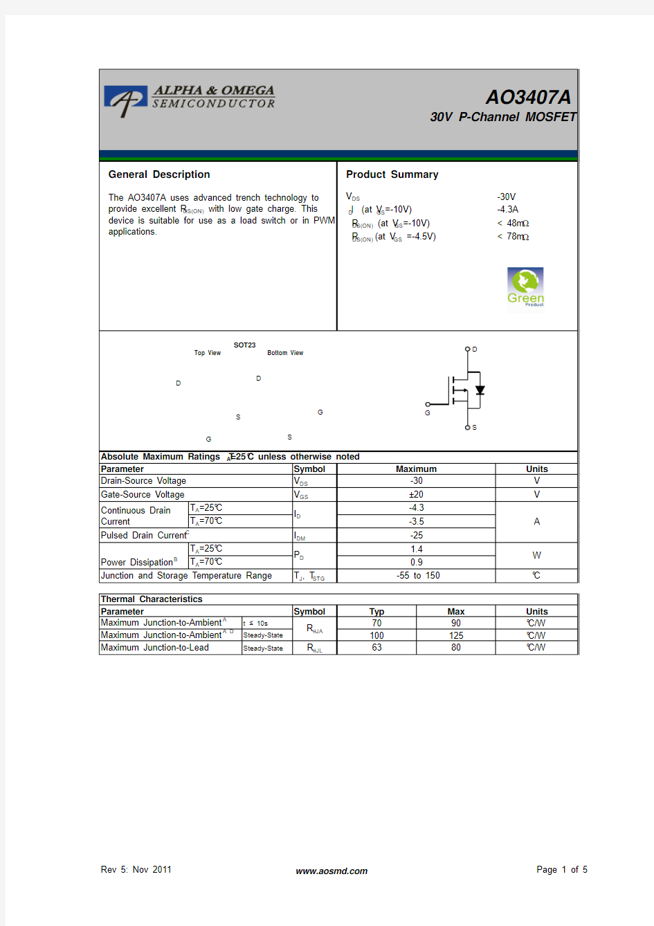
SOT23 Top View Bottom View
D
D
D
S G S
G
G S
Absolute Maximum Ratings TA=25° C unless otherwise noted Parameter Symbol VDS Drain-Source Voltage Gate-Source Voltage Continuous Drain Current Pulsed Drain Current C TA=25° C Power Dissipation B TA=70° C Junction and Storage Temperature Range Thermal Characteristics Parameter Maximum Junction-to-Ambient A Maximum Junction-to-Ambient A D Maximum Junction-to-Lead TA=25° C TA=70° C VGS ID IDM PD TJ, TSTG
Maximum -30 ±20 -4.3 -3.5 -25 1.4 0.9 -55 to 150
Units V V A
W ° C
Symbol
t ≤ 10s Steady-State Steady-State
RθJA RθJL
Typ 70 100 63
Max 90 125 80
Units ° C/W ° C/W ° C/W
Rev 5: Nov 2011
https://www.sodocs.net/doc/179801218.html,
Page 1 of 5
AO3407A
C unless otherwise noted) Electrical Characteristics (TJ=25° Symbol Parameter Conditions ID=-250μA, VGS=0V VDS=-30V, VGS=0V C TJ=55° VDS=0V, VGS= ±20V VDS=VGS ID=-250μA VGS=-10V, VDS=-5V VGS=-10V, ID=-4.3A RDS(ON) gFS VSD IS Static Drain-Source On-Resistance VGS=-4.5V, ID=-3A Forward Transconductance Diode Forward Voltage VDS=-5V, ID=-4.3A IS=-1A,VGS=0V TJ=125° C -1.4 -25 34 52 54 10 -0.7 -1 -2 520 VGS=0V, VDS=-15V, f=1MHz VGS=0V, VDS=0V, f=1MHz 3.5 100 65 7.5 9.2 VGS=-10V, VDS=-15V, ID=-4.3A 4.6 1.6 2.2 7.5 VGS=-10V, VDS=-15V, RL=3.5?, RGEN=3? IF=-4.3A, dI/dt=100A/μs 5.5 19 7 11 5.3 11.5 11 6 48 68 78 -1.9 Min -30 -1 -5 ±100 -2.4 Typ Max Units V μA nA V A m? m? S V A pF pF pF ? nC nC nC nC ns ns ns ns ns nC
STATIC PARAMETERS BVDSS Drain-Source Breakdown Voltage IDSS IGSS VGS(th) ID(ON) Zero Gate Voltage Drain Current Gate-Body leakage current Gate Threshold Voltage On state drain current
Maximum Body-Diode Continuous Current
DYNAMIC PARAMETERS Input Capacitance Ciss Coss Crss Rg Output Capacitance Reverse Transfer Capacitance Gate resistance
SWITCHING PARAMETERS Qg(10V) Total Gate Charge Qg(4.5V) Total Gate Charge Qgs Qgd tD(on) tr tD(off) tf trr Qrr Gate Source Charge Gate Drain Charge Turn-On DelayTime Turn-On Rise Time Turn-Off DelayTime Turn-Off Fall Time Body Diode Reverse Recovery Time Body Diode Reverse Recovery Charge IF=-4.3A, dI/dt=100A/μs
A. The value of RθJA is measured with the device mounted on 1in2 FR-4 board with 2oz. Copper, in a still air environment with TA =25°C. The value in any given application depends on the user's specific board design. B. The power dissipation PD is based on TJ(MAX)=150°C, using ≤ 10s junction-to-ambient thermal resistance. C. Repetitive rating, pulse width limited by junction temperature TJ(MAX)=150°C. Ratings are based on low frequency and duty cycles to keep initialTJ=25°C. D. The RθJA is the sum of the thermal impedence from junction to lead RθJL and lead to ambient. E. The static characteristics in Figures 1 to 6 are obtained using <300μs pulses, duty cycle 0.5% max. F. These curves are based on the junction-to-ambient thermal impedence which is measured with the device mounted on 1in2 FR-4 board with 2oz. Copper, assuming a maximum junction temperature of TJ(MAX)=150°C. The SOA curve provides a single pulse rating.
THIS PRODUCT HAS BEEN DESIGNED AND QUALIFIED FOR THE CONSUMER MARKET. APPLICATIONS OR USES AS CRITICAL COMPONENTS IN LIFE SUPPORT DEVICES OR SYSTEMS ARE NOT AUTHORIZED. AOS DOES NOT ASSUME ANY LIABILITY ARISING OUT OF SUCH APPLICATIONS OR USES OF ITS PRODUCTS. AOS RESERVES THE RIGHT TO IMPROVE PRODUCT DESIGN, FUNCTIONS AND RELIABILITY WITHOUT NOTICE.
Rev 5: Nov 2011
https://www.sodocs.net/doc/179801218.html,
Page 2 of 5
AO3407A
TYPICAL ELECTRICAL AND THERMAL CHARACTERISTICS
30 25 -10V 20 -ID (A) 15 -4V 10 5 0 0 1 2 3 4 5 -VDS (Volts) Fig 1: On-Region Characteristics (Note E) 80 Normalized On-Resistance 70 60 RDS(ON) (m? ) 50 40 30 20 10 0 6 8 10 -ID (A) Figure 3: On-Resistance vs. Drain Current and Gate Voltage (Note E) 2 4 VGS=-10V VGS=-4.5V VGS=-3.5V 10 5 0 0.5 1.5 2.5 3.5 4.5 5.5 -VGS(Volts) Figure 2: Transfer Characteristics (Note E) 125°C 25°C -4.5V 20 -ID(A) 15 -6V 25 30 VDS=-5V
1.8 1.6 1.4 1.2 1 0.8 0 25 50 75 100 125 150 175 VGS=-10V ID=-4.3A
VGS ID=-3A
17 5 2 10 =-4.5V
0 Temperature (° C) Figure 4: On-Resistance vs. Junction Temperature 18 (Note E)
120 ID=-4.3A 100 RDS(ON) (m? )
1.0E+02 1.0E+01 1.0E+00 -IS (A)
40
80 125°C 60
125°C 1.0E-01 1.0E-02 1.0E-03
25°C
40
25°C
1.0E-04 1.0E-05
20 6 8 10 -VGS (Volts) Figure 5: On-Resistance vs. Gate-Source Voltage (Note E) 2 4
0.0
0.2
0.4
0.6
0.8
1.0
1.2
-VSD (Volts) Figure 6: Body-Diode Characteristics (Note E)
Rev 5: Nov 2011
https://www.sodocs.net/doc/179801218.html,
Page 3 of 5
AO3407A
TYPICAL ELECTRICAL AND THERMAL CHARACTERISTICS
10 VDS=-15V ID=-4.3A 600 6 Capacitance (pF) -VGS (Volts) Ciss 800
8
400
4
Coss 200
2 Crss 0 5 10 15 20 25 -VDS (Volts) Figure 8: Capacitance Characteristics 30
0 0 2 4 6 8 Qg (nC) Figure 7: Gate-Charge Characteristics 10
0
100.0
40 TA=25°C
10.0
10μs
Power (W)
30
ID (Amps)
RDS(ON) limited
1.0
100μs 1ms 10ms 10ms
20
0.1
TJ(Max)=150°C TA=25°C
10s DC
10
0.0 0.01 0.1 1 VDS (Volts) 10 100
0 0.0001 1 100 Pulse Width (s) Figure 10: Single Pulse Power Rating Junction-toAmbient (Note F) 0.01
Figure 9: Maximum Forward Biased Safe Operating Area (Note F)
10 Zθ JA Normalized Transient Thermal Resistance D=Ton/T TJ,PK=TA+PDM.ZθJA.RθJA 1 RθJA=125°C/W
In descending order D=0.5, 0.3, 0.1, 0.05, 0.02, 0.01, single pulse
0.1 PD 0.01 Single Pulse Ton 0.001 0.00001 0.0001 0.001 0.01 0.1 1 10 100 1000 Pulse Width (s) Figure 11: Normalized Maximum Transient Thermal Impedance (Note F) PD Ton T T
Rev 5: Nov 2011
https://www.sodocs.net/doc/179801218.html,
Page 4 of 5
AO3407A
Gate Charge Test Circuit & Waveform
Vgs Qg -10V
VDC
VDC
DUT Vgs Ig
Resistive Switching Test Circuit & Waveforms
RL Vds Vgs Vgs Rg DUT
VDC
Vgs Vds
Diode Recovery Test Circuit & Waveforms
Vds + DUT Vgs
t rr
Vds Isd Vgs Ig
L
VDC
+ Vdd -Vds
Rev 5: Nov 2011
+
Charge
ton td(on) tr t d(off) toff tf
+
-
-
+
-
Vds
Qgs
Qgd
Vdd
90%
10%
Q rr = - Idt
-Isd
-I F
dI/dt -I RM Vdd
https://www.sodocs.net/doc/179801218.html,
Page 5 of 5
MURS120T3G 系列规格书推荐
MURS120T3G Series, SURS8120T3G Series, NRVUS120VT3G Series Surface Mount Ultrafast Power Rectifiers MURS105T3G, MURS110T3G, MURS115T3G, MURS120T3G, MURS140T3G, MURS160T3G, SURS8105T3G, SURS8110T3G, SURS8115T3G, SURS8120T3G, SURS8140T3G, SURS8160T3G, NRVUS110VT3G, NRVUS120VT3G, NRVUS160VT3G Ideally suited for high voltage, high frequency rectification, or as free wheeling and protection diodes in surface mount applications where compact size and weight are critical to the system. Features ?Small Compact Surface Mountable Package with J?Bend Leads ?Rectangular Package for Automated Handling ?High Temperature Glass Passivated Junction ?Low Forward V oltage Drop (0.71 to 1.05 V Max @ 1.0 A, T J = 150°C)?NRVUS and SURS8 Prefixes for Automotive and Other Applications Requiring Unique Site and Control Change Requirements; AEC?Q101 Qualified and PPAP Capable ?These Devices are Pb?Free, Halogen Free/BFR Free and are RoHS Compliant Mechanical Characteristics: ?Case: Epoxy, Molded ?Weight: 95 mg (Approximately) ?Finish: All External Surfaces Corrosion Resistant and Terminal Leads are Readily Solderable ?Lead and Mounting Surface Temperature for Soldering Purposes: 260°C Max. for 10 Seconds ?Polarity: Polarity Band Indicates Cathode Lead ?ESD Rating: ?Human Body Model = 3B (> 8 kV) ?Machine Model = C (> 400 V)See detailed ordering and shipping information in the table on page 2 of this data sheet. ORDERING INFORMATION MARKING DIAGRAM See general marking information in the device marking table on page 2 of this data sheet. DEVICE MARKING INFORMATION ULTRAFAST RECTIFIERS 1.0 AMPERE, 50?600 VOLTS SMB CASE 403A https://www.sodocs.net/doc/179801218.html, A=Assembly Location* Y=Year WW=Work Week U1=Device Code x = A, B, C, D, G, or J G=Pb?Free Package AYWW U1x G G (Note: Microdot may be in either location) * The Assembly Location code (A) is front side optional. In cases where the Assembly Location is stamped in the package bottom (molding ejecter pin), the front side assembly code may be blank.
LM393 系列规格书推荐
LM393, LM393E, LM293, LM2903, LM2903E, LM2903V, NCV2903 Low Offset Voltage Dual Comparators The LM393 series are dual independent precision voltage comparators capable of single or split supply operation. These devices are designed to permit a common mode range?to?ground level with single supply operation. Input offset voltage specifications as low as 2.0 mV make this device an excellent selection for many applications in consumer, automotive, and industrial electronics. Features ?Wide Single?Supply Range: 2.0 Vdc to 36 Vdc ?Split?Supply Range: ±1.0 Vdc to ±18 Vdc ?Very Low Current Drain Independent of Supply V oltage: 0.4 mA ?Low Input Bias Current: 25 nA ?Low Input Offset Current: 5.0 nA ?Low Input Offset V oltage: 5.0 mV (max) LM293/393 ?Input Common Mode Range to Ground Level ?Differential Input V oltage Range Equal to Power Supply V oltage ?Output V oltage Compatible with DTL, ECL, TTL, MOS, and CMOS Logic Levels ?ESD Clamps on the Inputs Increase the Ruggedness of the Device without Affecting Performance ?NCV Prefix for Automotive and Other Applications Requiring Unique Site and Control Change Requirements; AEC?Q100 Qualified and PPAP Capable ?These Devices are Pb?Free, Halogen Free/BFR Free and are RoHS Compliant Figure 1. Representative Schematic Diagram (Diagram shown is for 1 comparator)See detailed marking information and ordering and shipping information on pages 6 and 7 of this data sheet. DEVICE MARKING AND ORDERING INFORMATION PDIP?8 N SUFFIX CASE 626 8 SOIC?8 D SUFFIX CASE 751 1 PIN CONNECTIONS (Top View) Inputs A Inputs B Output B CC https://www.sodocs.net/doc/179801218.html, Micro8E DM SUFFIX CASE 846A 1
DSK32 SOD-123FL系列规格书推荐
DSK32 THRU DSK310SURFACE MOUNT SCHOTTKY BARRIER RECTIFIER Reverse Voltage - 20 to 100 Volts Forward Current -3.0 Ampere 1of 2
RATINGS AND CHARACTERISTIC CURVES DSK32 THRU DSK310 FIG. 3-TYPICAL INSTANTANEOUS FORWARD CHARACTERISTICS NUMBER OF CYCLES AT 60 Hz FIG. 2-MAXIMUM NON-REPETITIVE PEAK FORWARD FIG. 1- FORWARD CURRENT DERATING CURVE A V E R A G E F O R W A R D R E C T I F I E D C U R R E N T ,A M P E R E S I N S T A N T A N E O U S F O R W A R D C U R R E N T ,A M P E R E S P E A K F O R W A R D S U R G E C U R R E N T ,A M P E R E S INSTANTANEOUS FORWARD VOLTAGE, VOLTS 100 10 1 0.1 0.010.001 PERCENT OF PEAK REVERSE VOLTAGE,% FIG. 4-TYPICAL REVERSE CHARACTERISTICS I N S T A N T A N E O U S R E V E R S E C U R R E N T ,M I L L I A M P E R E S AMBIENT TEMPERATURE, C 2of 2
整流桥KBP310K KBP系列规格书推荐
KBP3005K THRU KBP310K SILICON BRIDGE RECTIFIERS Reverse Voltage - 50 to 1000 Volts Forward Current -3.0 Amperes
RATINGS AND CHARACTERISTIC CURVES KBP3005K THRU KBP310K 1.0 2.0 3.0 50 100 150 I ,A V E R A G E R E C T I F I E D C U R R E N T (A ) O T,TEMPERATURE (°C) 10 100 C , J U N C T I O N C A P A C I T A N C E (p F ) j V , REVERSE VOLTAGE (V) Fig. 4Typical Junction Capacitance R 00.1 1.0 10 0.2 0.4 0.6 0.8 1.0 1.2 1.4 I ,I N S T A N T A N E O U S F W D C U R R E N T (A ) F V ,INSTANTANEOUS FWD VOL TAGE (V) Fig.2T ypical Fwd Characteristics F Fig. 1 Forward Current Derating Curve Fig.3Max Non-Repetitive P eak Fwd Surge Current 50 40 100 30 I F S M ,P E A K F W D S U R G E C U R R E N T (A ) 10 NUMBER OF CYCLES AT 60 Hz 60 100
DSK18 SOD-123FL系列规格书推荐
DSK12 THRU DSK120 SURFACE MOUNT SCHOTTKY BARRIER RECTIFIER Reverse Voltage - 20 to 200 Volts Forward Current - 1.0 Ampere
1 0.8 0.6 0.4 0.2 FIG. 3-TYPICAL INSTANTANEOUS FORWARD CHARACTERISTICS NUMBER OF CYCLES AT 60 Hz FIG. 2-MAXIMUM NON-REPETITIVE PEAK FORWARD SURGE CURRENT FIG. 1- FORWARD CURRENT DERATING CURVE A V E R A G E F O R W A R D R E C T I F I E D C U R R E N T ,A M P E R E S I N S T A N T A N E O U S F O R W A R D C U R R E N T ,A M P E R E S P E A K F O R W A R D S U R G E C U R R E N T ,A M P E R E S INSTANTANEOUS FORWARD VOLTAGE, VOLTS 100 10 1 0.1 0.010.001 PERCENT OF PEAK REVERSE VOLTAGE,% FIG. 4-TYPICAL REVERSE CHARACTERISTICS I N S T A N T A N E O U S R E V E R S E C U R R E N T ,M I L L I A M P E R E S AMBIENT TEMPERATURE, C REVERSE VOLTAGE,VOLTS FIG. 5-TYPICAL JUNCTION CAPACITANCE J U N C T I O N C A P A C I T A N C E , p F 10 100 1000 2000RATINGS AND CHARACTERISTIC CURVES DSK12 THRU DSK120
SRLT系列产品规格书
S R L T系列产品规格书集团标准化工作小组 [Q8QX9QT-X8QQB8Q8-NQ8QJ8-M8QMN]
深圳硕日新能源科技有限公司 ShenZhen ShuoRi New Energy Technology Co.,Ltd 产品规格书 产品型号:SR-2LT 文件编号: 版本编号: 发行日期:2010-3-20 制定审核批准 地址:深圳市宝安区西乡鹤洲恒丰工业城C6栋 电话:5 传真:8 网址:
目录
1 产品规格 1.1 产品简介 本控制器专为太阳能路灯系统设计,太阳能庭院灯系统设计,具有两路负载输出,每路可分别实现双时段晨亮功能。同时具有丰富的参数设置,用户可以设置光控点电压、光控判断时间、延时开灯时间、蓄电池类型等,可根据实际环境设置不同参数,使系统达到最优设置。本产品支持铅酸电池、开口电池、胶体电池、锂铁电池等各种电池的使用,应用范围十分广泛。同时加入先进的自学习算法,能够自动识别夜晚长度,智能的调节二次开灯时间,使定时控制更加精确。本产品特有测试按键,方便安装调试使用。系统具有短路、过载、和独特的防反接保护,充满、过放自动关断、恢复等全功能保护措施,详细的充电指示、蓄电池状态、负载及各种故障指示。本控制器通过电脑芯片对蓄电池电压、光电池电压、放电电流、环境温度等参数进行采样,通过专用控制模型计算,实现符合蓄电池特性的放电率、温度补偿修正的高准确控制,并采用了智能高效的PWM 模糊充电方式对蓄电池进行充电,采用7段式电压控制,保证蓄电池工作在最佳状态,大大延长了蓄电池的使用寿命。对于具有自动识别的型号,系统上电时将检测系统电压,如果是12V 系统数码管显示“12”;如果是24V 系统数码管将显示“24”。 1.2 产品型号识别 SR – 2 L T 24 10 A 额定输出电流 自动识别型号 额定输入电压 产品功能代码,T 表示双时段系列 产品型号代码,2L 表示双路系列 硕日产品型号
贴片功率电感SWPA4030S330MT 系列规格书推荐
Wire Wound SMD Power Inductors – SWPA Series Operating temperature range: -40℃~+125℃ (Including self-heating) FEATURES ● Magnetic-resin shielded construction reduces buzz noise to ultra-low levels ● Metallization on ferrite core results in excellent shock resistance and damage-free durability ● Closed magnetic circuit design reduces leakage flux and Electro Magnetic Interference (EMI) ● 30% higher current rating than conventional inductors of equal size ● Takes up less PCB real estate and save more power APPLICATIONS ● Smart phone, smart TV, set top box, notebook ● Car navigation systems, telecomm base stations ● VR, AR ● LED lighting PRODUCT IDENTIFICATION SWPA 3012 S 1R0 N T □□□ ① ② ③ ④ ⑤ ⑥ ⑦ ② External Dimensions (L×W×H) [mm] 252010 2.5×2.0×1.0 252012 2.5×2.0×1.2 3010 3.0×3.0×1.0 3012 3.0×3.0×1.2 3015 3.0×3.0×1.5 4010 4.0×4.0×1.0 4012 4.0×4.0×1.2 4018 4.0×4.0×1.8 4020 4.0×4.0×2.0 4026 4.0×4.0×2.6 4030 4.0×4.0×3.0 5012 5.0×5.0×1.2 5020 5.0×5.0×2.0 5040 5.0×5.0×4.0 6020 6.0×6.0×2.0 6028 6.0×6.0×2.8 6040 6.0×6.0×4.0 6045 6.0×6.0×4.5 8040 8.0×8.0×4.0 8050 8.0×8.0×5.0 8060 8.0×8.0×6.0 8065 8.0×8.0×6.5 ① Type SWPA Wire Wound SMD Power Inductor ③ Feature Type S Standard ④ Nominal Inductance Example Nominal Value 1R0 1.0μH 100 10μH ⑤ Inductance Tolerance K ±10% M ±20% N ±30% ⑥ Packing T Tape Carrier Package ⑦ Design Code □□□ Standard product is blank https://www.sodocs.net/doc/179801218.html,
TEAPO_SC系列规格书
■ Features: 105℃ at high frequency and high operation temperature (-40 ~ +105℃)■ Recommended Applications: Applicable for switching regulator of computer ,■Corresponding product to RoHS ψD 58101213161822P 2.0 3.5 5.0 5.0 5.07.57.510.0ψd 0.500.6 0.60.60.60.80.80.8 ( 1.0 )a 1.5 1.5 1.5 2.0 2.0 2.0 2.0 2.0 ■ Multiplier for Ripple Current Frequency (Hz)Below 4.7 μF 5.6 ~ 33 μF 34 ~ 330 μF 331 ~ 1000 μF 1200 μF Above 1.00 especially for high frequency 0.85 0.900.950.98 1.000.950.60 1.00 1.000.900.90 1.000.400.500.650.900.900.980.700.80 1.000.400.500.600.800.300.700.80501203001K 10K 100K 1.006.32.5 Frequency coefficient 1.5■ Diagram of Dimensions 0.5Series ( ) : L ≧40
SIZE Ripple Z SIZE Ripple Z SIZE Ripple Z SIZE Ripple Z 4.76.85x11500.550 2233475x111500.450565x111000.6305x111500.420685x111500.420 6.3x112000.3705x111500.4205x112000.370 6.3x112500.2201205x11 2000.370 6.3x112500.3208x113000.2001505x112000.420 6.3x112500.320 6.3x113000.2208x115500.1406.3x112500.320 6.3x11 300 0.220 8x11 550 0.140 *8x116200.1208x157500.100270*6.3x113000.220*6.3x113200.2308x115500.140 *8x116200.120*8x156600.1008x114000.1808x157500.1008x208000.06910x12.56880.08010x169000.086*6.3x114400.180*8x116200.120*8x157300.093*8x2010000.0678x115500.1408x157500.10010x12.58000.085*10x12.59000.08610x1610500.064*8x115800.120*8x116400.11010x1610500.06410x2011000.0398x157000.10010x12.58000.0858208x207500.08510x1610500.06410x2011000.04410x2012500.039*8x115800.1508x2010800.065*10x1611400.043*10x2011600.047*8x156700.085*10x12.59300.07510x20 1250 0.039 *10x2513100.0428x208000.06910x169900.08513x2014500.03810x12.56900.08010x2011000.05010x1610000.06410x2012500.044*10x2513100.04213x2516000.29013x2014500.038*8x159800.08510x20 1450 0.039 *10x2012000.045*12x3017500.032*8x2010700.05113x2016000.034 16x25 2000 0.028 *10x1610700.05510x2012500.044*10x2012200.051*10x2013300.047*10x3017800.032*13x3018100.029*10x2513100.048*10x2514500.039*13x2017200.033*16x2516600.03213x2014500.04313x2016000.03813x2520000.02816x3222000.024*10x2514000.043*10x3017400.032*13x4022000.026*16x3625400.01913x2517000.03513x2520000.02816x2522000.02418x3625500.019390013x2517500.032*12x3015700.033*13x2518600.02816x36 2550 0.019 18x36 2800 0.019 *13x2515200.03216x2522000.02416x2518000.028680016x3220000.02416x3625500.01918x3628000.01918x3628000.019 820016x3223500.01918x36 2800 0.019 1000016x3625500.01915000 18x36 3000 0.019 " * " is down size , Ripple Life is less 1000 hrs than standard Rated ( Surge) Voltage Capacitance (μF) 330 2200 3300 ☆ Size: D ψx L (mm) ☆ Ripple Current: (mA/rms), 105℃,100KHz ☆Impedance (Ω),20℃,100KHz 470025V ( 32 ) 10100220470 1500 1000 6801200 ■Dimensions,Rated Ripple Current,Max Impedance 10V ( 13 )6.3V ( 8 ) 16V ( 20 )
光纤FC系列规格书
XXX通讯设备有限公司 FC 系列产品 规格书 (文件编号: XXX-PSEN-0001) 版本:1.0 2015年03月 编制:审核:批准:
目录 1.应用范围‥‥‥‥‥‥‥‥‥‥‥‥‥‥‥‥‥‥‥‥‥‥1 2.FC系列跳线‥‥‥‥‥‥‥‥‥‥‥‥‥‥‥‥‥‥‥‥1 2.1 材质‥‥‥‥‥‥‥‥‥‥‥‥‥‥‥‥‥‥‥‥‥‥‥1 2.2 规格、尺寸‥‥‥‥‥‥‥‥‥‥‥‥‥‥‥‥‥‥‥‥1 2.3 性能指标‥‥‥‥‥‥‥‥‥‥‥‥‥‥‥‥‥‥‥‥‥9 2.4 实验内容‥‥‥‥‥‥‥‥‥‥‥‥‥‥‥‥‥‥‥‥‥10 2.5 产品图片‥‥‥‥‥‥‥‥‥‥‥‥‥‥‥‥‥‥‥‥‥12 3.FC一体式适配器‥‥‥‥‥‥‥‥‥‥‥‥‥‥‥‥‥‥ 12 3.1 材质‥‥‥‥‥‥‥‥‥‥‥‥‥‥‥‥‥‥‥‥‥‥‥12 3.2 规格、尺寸‥‥‥‥‥‥‥‥‥‥‥‥‥‥‥‥‥‥‥‥13 3.3 性能指标‥‥‥‥‥‥‥‥‥‥‥‥‥‥‥‥‥‥‥‥‥14 1.应用范围 本规格书适用于FC型光纤活动连接器(跳线、适配器)的生产、检验和使用 FC型光纤活动连接器是一种以单芯插头和适配器为基础组成的螺纹旋转式连接器,它的特点是光纤镶嵌在标称直径为2.5mm的高精密插针圆柱体中,两插头用M8×0.75的螺帽和适配器进行螺纹连接。 使用条件: 工作温度:-25℃——+70℃ 贮运温度:-40℃——+85℃ 相对湿度:不大于95%(+40℃时) 大气压力:70Kpa——106Kpa 2.FC系列跳线、尾纤 2.1 材质 金属件:弹簧、外螺、内框、止动环、喇叭口、压环、尾座 陶瓷件:插芯 塑料件:尾套、防尘帽 光缆:二氧化硅、芳族聚酸胺、聚氯乙烯 如需符合ROHS,需在评审单上注明。
A-25GA产品规格书
● 产品特性 -25~+70℃工作温度(具体查看降额曲线) 短路/过载/过压保护功能 100%满载老化 效率高、高可靠性 2年质保期 ● 应用领域:工业控制系统、机械与电气设备、电子仪器仪表、工业自动化、家用电器等 ● 参考标准 EN55024\EN61000-4-2,3,4,5,6,8,11\GB17625.1\EN61000-3-2,-3\EN55022\GB4943\UL1012 ● 产品描述 A-25GA 系列是一款25W 单路恒压输出的工业控制电源,电压输入范围176~264VAC ,输出电压有5V 、12V 、24V 等,可适用于工业控制系统、机械与电气设备、电子仪器仪表、工业自动化、家用电器等多种工业领域。超高的效率,紧凑的外壳设计,良好的散热,保障了本系列产品可长期稳定的工作。 ● 产品命名
电气参数
输出负载与温度曲线 静态特性曲线 机构尺寸
●安装方式 ●产品安装、使用说明: 1、安装时,请按照安装方式说明进行安装。 2、在安装完毕通电试运行之前,请检查和校对各接线端子上的连线,确信输入和输出、交流和直流、正极和负极、电压值和电流值等正确,杜绝接反接错现象的发生,避免损坏电源和用户设备。 3、通电前请使用万用表测量火线、零线和接地线是否短路,输出端是否短路;通电时最好空载启动。 4、使用时请勿超过电源标称值,以免影响产品的可靠性。如需更改电源的输出参数,请客户在使用电源前向本司技术部门咨询,以保证使用效果和可靠性。 5、为保证使用的安全性和减小干扰,请确保接地端可靠接地(接地线大于AWG18#)。 6、电源如出现故障,请勿擅自对其维修,请尽快与本司客户服务部联系,客服专线:86-519-85215050。 ●运输、储存: 1、运输: 本包装适用与汽车、船、飞机、火车等运输,运输过程中应防雨,文明装卸。 2、储存: 产品未使用时应放在包装箱里,储存环境温度和相对湿度应符合该产品的要求,仓库内不应有腐蚀性气体或产品,并且无强烈的机械振动、冲击和强磁场作用。包装箱应垫离地面至少20cm高,勿让水浸。如果储存时间过长(1年以上)应经专业人员重新检验后方可使用。
相关文档
- M1-M7 DO-214AC SMAJ 系列规格书推荐
- MB4S 封装MBS 系列规格书推荐
- MB6S 封装MBS 系列规格书推荐
- TL431A TL431B 系列规格书推荐
- DSK32 SOD-123FL系列规格书推荐
- DSK36 SOD-123FL系列规格书推荐
- DSK19 SOD-123FL系列规格书推荐
- KBP2005 KBP 系列规格书推荐
- LM393 系列规格书推荐
- 整流桥KBP304K KBP系列规格书推荐
- LM324系列 LM224 LM324规格书推荐
- 贴片功率电感SWPA4030S330MT 系列规格书推荐
- LR2728-24R040F1系列规格书贴片合金电阻推荐
- KBP2010 KBP 系列规格书推荐
- MB2S 封装MBS 系列规格书推荐
- MB1S-MB10S封装MBS 系列规格书推荐
- MC33078 MC33079 系列规格书推荐
- 整流桥KBP302K KBP系列规格书推荐
- MURS120T3G 系列规格书推荐
- DSK110 SOD-123FL系列规格书推荐