HD74LS273P中文资料

HD74LS273
Octal D-type Positive-edge-triggered Flip-Flops (with Clear)
REJ03D0473–0300
Rev.3.00 Jul.15.2005
The HD74LS273, positive-edge-triggered flip-flops utilize LS TTL circuitry to implement D-type flip-flop logic with a direct clear input.
Information at the D inputs meeting the setup time requirements is transferred to the Q outputs on the positive-going edge of the clock pulse.
When the clock input is at either the high or low level, the D input signal has no effect at the output.
Features
? Ordering Information
Part Name
Package Type
Package Code (Previous Code) Package
Abbreviation
Taping Abbreviation (Quantity)
HD74LS273P DILP-20 pin PRDP0020AC-B (DP-20NEV) P — HD74LS273FPEL SOP-20 pin (JEITA) PRSP0020DD-B (FP-20DAV)
FP
EL (2,000 pcs/reel) HD74LS273RPEL SOP-20 pin (JEDEC)
PRSP0020DC-A
(FP-20DBV)
RP
EL (1,000 pcs/reel)
Note: Please consult the sales office for the above package availability.
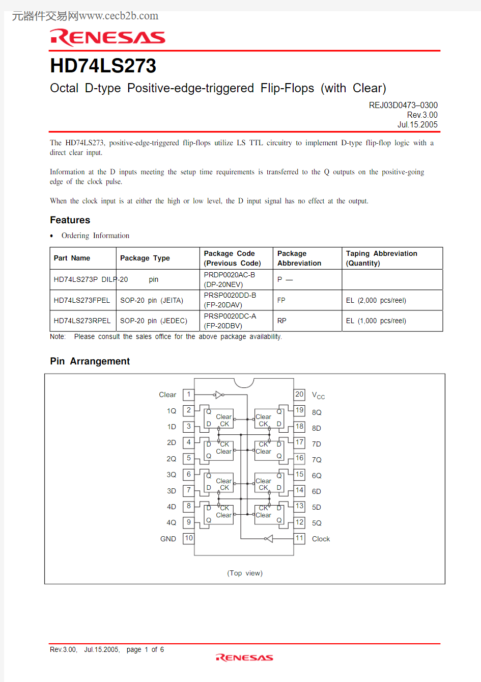
Pin Arrangement
Function Table
Inputs Output Clear Clock D Q
L X X L
H ↑ H H
H ↑ L L
H L X Q0
Notes: H; high level, L; low level, X; irrelevant
↑; transition from low to high level
Q0; level of Q before the indicated steady-state input conditions were established.
Block Diagram
Absolute Maximum Ratings
Unit
Ratings
Item Symbol
Supply voltage V CC 7 V
Input voltage V IN 7 V
Power dissipation P T 400 mW
Storage temperature Tstg –65 to +150 °C
Note: Voltage value, unless otherwise noted, are with respect to network ground terminal.
Recommended Operating Conditions
Max
Typ
Unit
Min
Item Symbol
Supply voltage V CC 4.75 5.00 5.25 V
I OH — — –400 μA
Output current
I OL — — 8 mA
°C
75
Operating temperature Topr
25
–20
Clock frequency ?clock 0 — 30 MHz
Clock pulse width t w (clock) 20 — — ns
Clear pulse width t w (clear) 20 — — ns
Data setup time t su (data) 20↑ — — ns
Clear (inactive-state) setup time t su (clear) 25↑ — — ns
Data hold time t h (data)5↑ — — ns
Electrical Characteristics
(Ta = –20 to +75 °C)
Item Symbol min. typ.* max. Unit
Condition
V IH 2.0 — — V
Input voltage
V IL — — 0.8 V
V OH 2.7 — — V
V CC = 4.75 V, V IH = 2 V, V IL = 0.8 V,
I OH = –400 μA
— — 0.5 I OL = 8 mA Output voltage
V OL — — 0.4 V
I OL = 4 mA V CC = 4.75 V, V IH = 2 V,
V IL = 0.8 V
I IH — 20 μA V CC = 5.25 V, V I = 2.7 V I IL — –0.4 mA V CC = 5.25 V, V I = 0.4 V
Input current
I I —
0.1 mA V CC = 5.25 V, V I = 7 V Short-circuit output current
I OS –20 — –100 mA V CC = 5.25 V Supply current
I CC ** — 17 27 mA V CC = 5.25 V Input clamp voltage V
IK — — –1.5 V V CC = 4.75 V, I IN = –18 mA
Notes: * V CC = 5 V, Ta = 25°C ** With all outputs open and 4.5 V applied to all data and clear inputs, I CC is measured after a momentary
ground, then 4.5 V is applied to clock.
Switching Characteristics
(V CC = 5 V, Ta = 25°C)
Item Symbol Inputs min. typ. max. Unit Condition
Maximum clock frequency ?max Clock 30 40 — MHz
t PHL Clear — 18 27
t PLH — 17 27
Propagation delay time t PHL Clock
— 18 27 ns C L = 15 pF, R L = 2 k ?
Testing Method
Test Circuit
Waveforms 1
Waveforms 2
Package Dimensions
https://www.sodocs.net/doc/f75831723.html, RENESAS SALES OFFICES
Refer to "https://www.sodocs.net/doc/f75831723.html,/en/network" for the latest and detailed information.
Renesas Technology America, Inc.
450 Holger Way, San Jose, CA 95134-1368, U.S.A
Tel: <1> (408) 382-7500, Fax: <1> (408) 382-7501
Renesas Technology Europe Limited
Dukes Meadow, Millboard Road, Bourne End, Buckinghamshire, SL8 5FH, U.K.
Tel: <44> (1628) 585-100, Fax: <44> (1628) 585-900
Renesas Technology Hong Kong Ltd.
7th Floor, North Tower, World Finance Centre, Harbour City, 1 Canton Road, Tsimshatsui, Kowloon, Hong Kong
Tel: <852> 2265-6688, Fax: <852> 2730-6071
Renesas Technology Taiwan Co., Ltd.
10th Floor, No.99, Fushing North Road, Taipei, Taiwan
Tel: <886> (2) 2715-2888, Fax: <886> (2) 2713-2999
Renesas Technology (Shanghai) Co., Ltd.
Unit2607 Ruijing Building, No.205 Maoming Road (S), Shanghai 200020, China
Tel: <86> (21) 6472-1001, Fax: <86> (21) 6415-2952
Renesas Technology Singapore Pte. Ltd.
1 Harbour Front Avenue, #06-10, Keppel Bay Tower, Singapore 098632
Tel: <65> 6213-0200, Fax: <65> 6278-8001
Renesas Technology Korea Co., Ltd.
Kukje Center Bldg. 18th Fl., 191, 2-ka, Hangang-ro, Yongsan-ku, Seoul 140-702, Korea
Tel: <82> 2-796-3115, Fax: <82> 2-796-2145
Renesas Technology Malaysia Sdn. Bhd.
Unit 906, Block B, Menara Amcorp, Amcorp Trade Centre, No.18, Jalan Persiaran Barat, 46050 Petaling Jaya, Selangor Darul Ehsan, Malaysia
Tel: <603> 7955-9390, Fax: <603> 7955-9510