mst706_Pb_v01
M
S t a r C o n f i d e n t i a l f o r S h e n z h e n s u n p r o t e c h n o l o g y c o .,l t d I n t e r n a l U s e O n l y
FEATURES
n
Video Decoder
? Supports NTSC, PAL and SECAM video input formats
? 2D NTSC and PAL comb-filter for Y/C separation of CVBS input
? ACC, AGC, and DCGC (Digital Chroma Gain Control)
n
Analog Input
? Supports video input 480i, 576i, On-chip clock synthesizer and PLL
n
Color Engine
? Brightness, contrast, saturation, and hue
adjustment
? 9-tap programmable multi-purpose FIR (Finite Impulse Response) filter
? Differential 3-band peaking engine
? Luminance Transient Improvement (LTI) ? Chrominance Transient Improvement (CTI) ? Black Level Extension (BLE) ? White Level Extension (WLE)
? Favor Color Compensation (FCC) ? 3-channel gamma curve adjustment
Miscellaneous
? Built-in MCU
? Built-in internal OSD with 256 programmable fonts, 16-color palettes, and 12-bit color resolution
? Spread spectrum clocks
? 3.3V output pads with programmable driving current ? 64-pin TQFP package
n
Scaling Engine/Panel Interface
? Supports TTL/TCON panel
? Supports single 8-bit TTL panel output ? Supports various displaying modes ? Supports horizontal panorama scaling
r C o t i a z h e n t e n o l o y c o .,l I n t e l U n l y
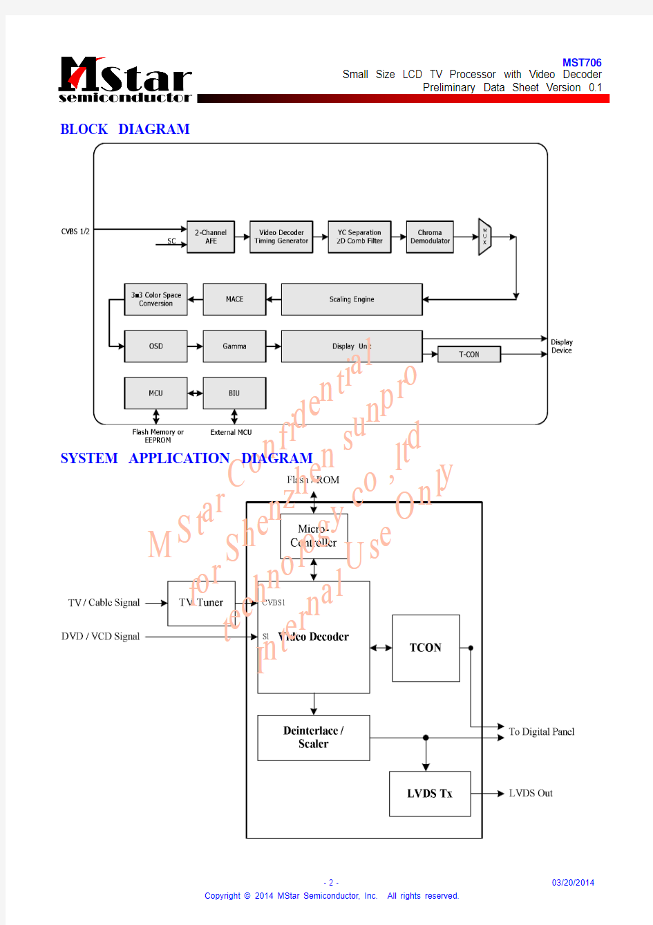
BLOCK DIAGRAM
SYSTEM APPLICATION DIAGRAM
M
S t a r C o n f i d e n t i a l f o r S h e n z h e n s u n p r o t e c h n o l o g y c o .,l t d I n t e r n a l U s e O n l y
GENERAL DESCRIPTION
The MST706 is a high quality ASIC for NTSC/PAL/SECAM car TV application. It receives analog
NTSC/PAL/SECAM CVBS and S-Video inputs from TV tuners, DVD or VCR sources, including weak and distorted signals, as well as analog YCbCr input from HDTV/SDTV systems. Automatic gain control (AGC) and 10-bit A/D converters provide high resolution video quantization. With automatic video source and mode detection, users can easily switch and adjust variety of signal sources. Multiple internal adaptive PLLs precisely extract pixel clock from video source and perform sharp color demodulation. Built-in line-buffer supports adaptive 2-D comb-filter, 2-D sharpening, and synchronization stabler in a condense manner. The output format of MST706 supports 6-bit TTL/TCON digital TFT-LCD modules.
n f i d e n z h e n s u g y c
PIN DIAGRAM (MST706)
ROUT[2]
ROUT[3]VDDP VCOM0AVDD_ANA
SAR0SAR1SAR2SCK SDI DPWN_IFB CVBS2/SY0CVBS1/SC0DPWM_QQR
VDDC GND SDO
AGND GOUT[1]GOUT[0]
ROUT[7]/TCON[6]]ROUT[6]/TCON[7]ROUT[5]ROUT[4]BOUT[0]GND
GOUT[7]/TCON[4]GOUT[6]/TCON[5]GOUT[5]GOUT[4]GOUT[3]GOUT[2]MST706-LF
XXXXXXXXXXX XXXXX
M
S t a r C o n f i d e n t i a l f o r S h e n z h e n s u n p r o t e c h n o l o g y c o .,l t d I n t e r n a l U s e O n l y
PIN DESCRIPTION Analog Interface
Pin Name Pin Type Function
Pin VCOM0 Analog Input Common Analog Input Reference Ground 0 3 CVBS1/SC0 Analog Input CVBS0 or S-Video (Y/C) Input Channel 0 4 CVBS2/SY0 Analog Input
CVBS1 or S-Video (Y/C) Input Channel 0
5
Internal MCU Interface with Serial Flash Memory
Pin Name Pin Type Function Pin SAR2 Analog Input SAR Low Speed ADC Input 2 13 SAR1 Analog Input SAR Low Speed ADC Input 1 12 SAR0 Analog Input SAR Low Speed ADC Input 0 11 SCK Output SPI Interface Sampling Clock 14 SDI Output SPI Interface Data-In 15 SDO Input w/ 5V-tolerant
SPI Interface Data-Out
16 CSN Output SPI Interface Chip Select 17 INT Input
Interrupt Input for IR Receiver
18 TXD_SDA I/O w/ 5V-tolerant, w/ pull-up resistor Serial Bus Data
19 RXD_SCL Input w/ 5V-tolerant
Serial Bus Clock
20 PWM1D
Output
Pulse Width Modulation Output; 4mA driving strength
26 GPIO[25]/PWM4D I/O w/ 5V-tolerant General Purpose Input/Output /
Pulse Width Modulation Output; 4mA driving strength 60 GPIO[24]/PWM3D I/O w/ 5V-tolerant
General Purpose Input/Output /
Pulse Width Modulation Output; 4mA driving strength
59
Digital Panel Output Interface
Pin Name Pin Type Function
Pin CLKO
Output Display Clock Output 25 DEO/TCON[10] Output Display Enable Output
24 VSYNCO/TCON[9] Output Vertical Sync Output / TCON Output[9]
23 HSYNCO/TCON[8]
Output
Horizontal Sync Output / TCON Output[8] 22 ROUT[7]/TCON[6] Output Red channel Output [7] / TCON Output[6] 38 ROUT[6]/TCON[7] Output Red channel Output [6] / TCON Output[7]
37
ROUT[5:0]
Output
Red channel Output [5:0]
36, 35, 34, 33, 32, 31
M
S t a r C o n f i d e n t i a l f o r S h e n z h e n s u n p r o t e c h n o l o g y c o .,l t d I n t e r n a l U s e O n l y
Pin Name
Pin Type
Function
Pin GOUT[7]/TCON[4] Output Green channel Output [7] / TCON Output[4]
46 GOUT[6]/TCON[5] Output Green channel Output [6] / TCON Output[5]
45
GOUT[5:0]
Output
Green channel Output [5:0]
44, 43, 42, 41, 40, 39
BOUT[7]/TCON[2] Output Blue channel Output [7] / TCON Output[2] 55 BOUT[6]/TCON[3] Output Blue channel Output [6] / TCON Output[3] 54 BOUT[5:0] Output Blue channel Output [5:0] 53, 52, 51, 50, 49, 48 TCON[1] Output
TCON Output[1]
56
GPIO Interface
Pin Name Pin Type
Function
Pin GPIOD I/O w/ 5V-tolerant General Purpose Input Output; 4mA driving strength 57 GPIOE I/O w/ 5V-tolerant General Purpose Input Output; 4mA driving strength
58
Digital PWM Interface
Pin Name Pin Type Function
Pin DPWM_IFB Analog Input
Input for DPWM Feedback Loop 6 DPWM_QOR Output
DPWM Output
7
Misc. Interface
Pin Name Pin Type
Function
Pin RESET Schmitt Trigger Input w/ 5V-tolerant Hardware Reset; active high 27 XTAL_IN Analog Input
Crystal Oscillator Input
63 XTAL_OUT Analog Output
Crystal Oscillator Output
62
Power Pins
Pin Name Pin Type Function Pin AVDD_ANA 3.3V Power Analog ADC Power 1 AVDD_MPLL 3.3V Power MPLL Power 64 VDDC 1.2V Power Digital Core Power 9, 28 VDDP 3.3V Power Digital Input/Output Power 8, 29 AGND Ground Analog Ground 2, 61 GND
Ground
Ground
10, 21, 30, 47
M
S t a r
C o n f i d e n t i a l
f o r
S h e n z h e n
s
u n p r o
t e c h n o l o g y c o .,l t d I n t e r n a l U s e O n l y
ELECTRICAL SPECIFICATIONS Absolute Maximum Ratings
Parameter
Symbol Min Max Units 3.3V Supply Voltages V VDD_33 3.63 V 1.2V Supply Voltages
V VDD_12 1.32 V Input Voltage (5V tolerant inputs) V IN5Vtol 5.0 V Input Voltage (non 5V tolerant inputs) V IN V VDD_33 V Ambient Operating Temperature T A 0 70 °C Storage Temperature T STG -40 125 °C Junction Temperature
T J
125
°C
Note: Stresses above those listed in Absolute Maximum Ratings may cause permanent damage to the device. This is a stress rating only and does not imply functional operation of the device. Exposure to absolute maximum ratings for extended periods may affect device reliability.
ORDERING GUIDE
Part Number
Temperature Range
Package
Description Package Option MST706-LF 0°C to +70°C
TQFP
64
MARKING INFORMATION
MST706-LF
DISCLAIMER
MSTAR SEMICONDUCTOR RESERVES THE RIGHT TO MAKE CHANGES WITHOUT FURTHER NOTICE TO ANY PRODUCTS HEREIN TO IMPROVE RELIABILITY, FUNCTION OR DESIGN. NO RESPONSIBILITY IS ASSUMED BY MSTAR SEMICONDUCTOR ARISING OUT OF THE APPLICATION OR USER OF ANY PRODUCT OR CIRCUIT DESCRIBED HEREIN; NEITHER DOES IT CONVEY ANY LICENSE UNDER ITS PATENT RIGHTS, NOR THE RIGHTS OF OTHERS.
REVISION HISTORY
Document Description Date MST706_pb_v01
? Initial release
03/20/2014
Electrostatic charges accumulate on both test equipment and human body and can discharge without detection. MST706 comes with ESD protection circuitry; however, the device may be permanently damaged when subjected to high energy discharges. The device should be handled with proper ESD precautions to prevent malfunction and performance degradation.
M
a r n z
t e c r n
MECHANICAL DIMENSIONS