OV519 Datasheet _v1.3
Advanced Information
OV519 C AMERA M ATE ? Processor
Enhanced Single Chip Processor for USB PC Camera Applications
General Description
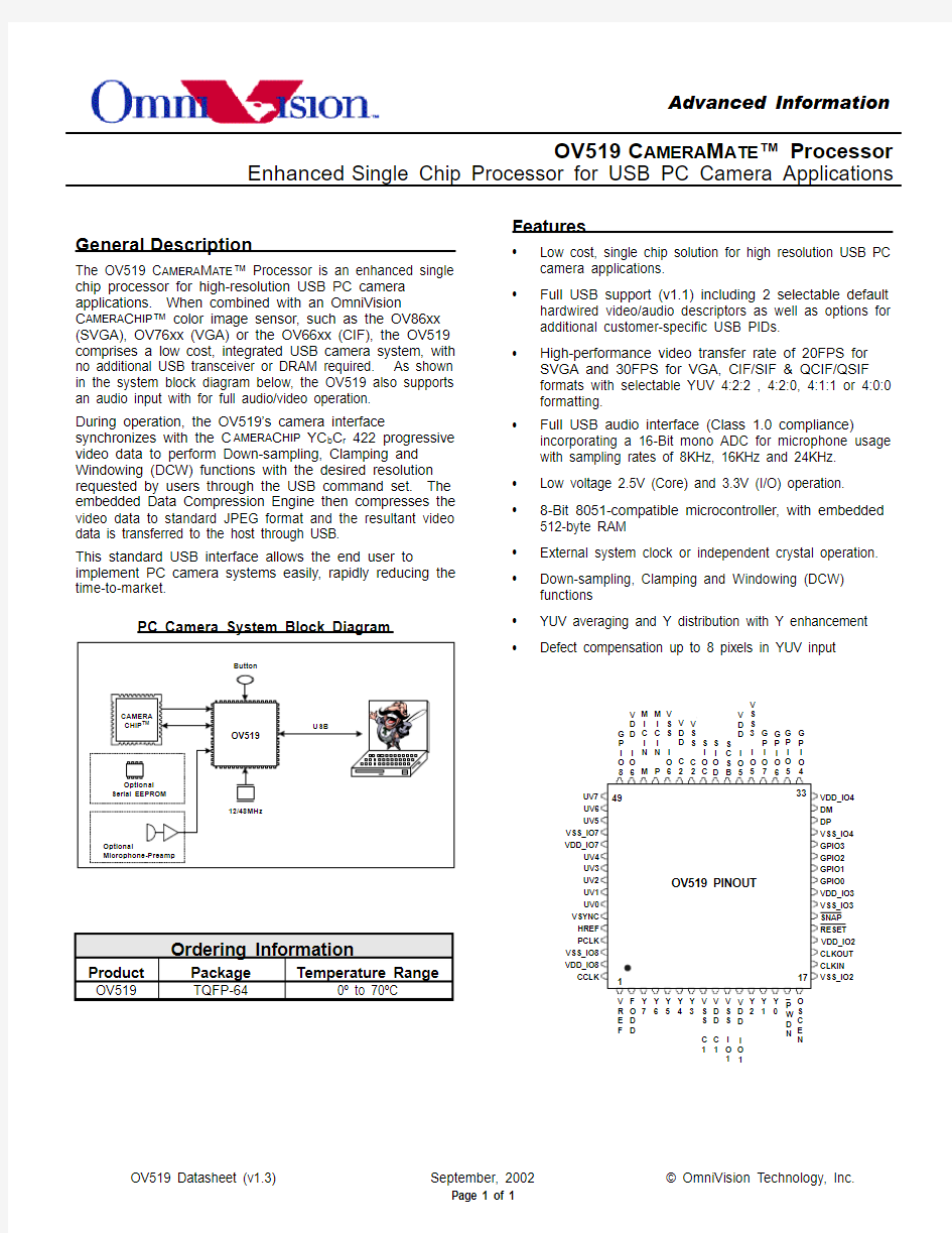
The OV519 C AMERA M ATE ? Processor is an enhanced single chip processor for high-resolution USB PC camera applications. When combined with an OmniVision C AMERA C HIP ? color image sensor, such as the OV86xx (SVGA), OV76xx (VGA) or the OV66xx (CIF), the OV519 comprises a low cost, integrated USB camera system, with no additional USB transceiver or DRAM required. As shown in the system block diagram below, the OV519 also supports an audio input with for full audio/video operation.
During operation, the OV519’s camera interface synchronizes with the C AMERA C HIP YC b C r 422 progressive video data to perform Down-sampling, Clamping and Windowing (DCW) functions with the desired resolution requested by users through the USB command set. The embedded Data Compression Engine then compresses the video data to standard JPEG format and the resultant video data is transferred to the host through USB.
This standard USB interface allows the end user to implement PC camera systems easily, rapidly reducing the time-to-market.
PC Camera System Block Diagram
Ordering Information
Product
Package
Temperature Range
OV519
TQFP-64
0o to 70oC
Features
? Low cost, single chip solution for high resolution USB PC
camera applications.
?
Full USB support (v1.1) including 2 selectable default hardwired video/audio descriptors as well as options for additional customer-specific USB PIDs.
?
High-performance video transfer rate of 20FPS for SVGA and 30FPS for VGA, CIF/SIF & QCIF/QSIF formats with selectable YUV 4:2:2 , 4:2:0, 4:1:1 or 4:0:0 formatting.
?
Full USB audio interface (Class 1.0 compliance) incorporating a 16-Bit mono ADC for microphone usage with sampling rates of 8KHz, 16KHz and 24KHz. ? Low voltage 2.5V (Core) and 3.3V (I/O) operation. ? 8-Bit 8051-compatible microcontroller, with embedded 512-byte RAM
? External system clock or independent crystal operation. ? Down-sampling, Clamping and Windowing (DCW) functions
? YUV averaging and Y distribution with Y enhancement ?
Defect compensation up to 8 pixels in YUV input
R E F
O D
D
76543S S C 1D
D C 1
S S I O 1D D I
O 1
210P W D N S C
E N G P I O G P I O G P I O G
P I O V S S 3I O V D D I O S C S S I O S I O V S
S C 2
V D D C V
S S I
O M I C
I N V D D I O
G P
I O M I C I N
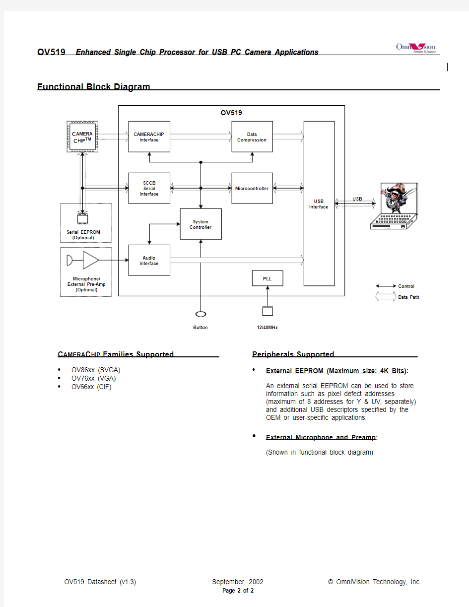
Functional Block Diagram
12/48MHz
Button
C AMERA C HIP Families Supported ? OV86xx (SVGA)
? OV76xx (VGA)
? OV66xx (CIF) Peripherals Supported
? External EEPROM (Maximum size: 4K Bits): An external serial EEPROM can be used to store information such as pixel defect addresses
(maximum of 8 addresses for Y & UV, separately) and additional USB descriptors specified by the
OEM or user-specific applications.
? External Microphone and Preamp:
(Shown in functional block diagram)
Function Block Details
? C AMERA C HIP Interface:
The camera data interface supports both 8-bit and 16-bit data widths at clock speeds up to 48MHz, as a function of the camera chip used.
? Audio Interface:
The audio input accepts the output of a microphone/pre-amp and converts it to a 16 Bit digital datastream with user-selected sampling rates of 8KHz, 16KHz or 24KHz. This digital audio data is then transferred to the PC system through the USB interface, providing full video & audio to the end user.
? Microcontroller:
The microcontroller operates as an embedded controller only and can be programmed by the user if custom applications are desired. Please contact OmniVision for further information on microcontroller implementation.
? System Controller:
This function provides general system control to the internal logic. This includes all clock and reset signals and functions such as controlling the USB Power-Down SUSPEND mode and GPIO (General Purpose I/O) configuration, which can allow the user to control external peripherals.
? Data Compression:
The OV519 uses a standard JPEG compression engine to transmit high-resolution images at video rates.
? SCCB Serial Interface:
The SCCB interface controls the C AMERA C HIP operation as well as interfacing to the optional EEPROM. In all cases, the OV519 is considered the SCCB ‘Master’ and all other SCCB devices, such as the C AMERA C HIP or optional EEPROM, are designated as ‘Slaves’.
Note: The description below is a functional overview on the interface. For a complete description, please refer to Application Note ‘AN101 – SCCB Functional Specification’.
SCCB WRITE (To Slave) Transmission:
BYTE (Register) WRITE
7 6 5 4 3 2 1 0 X 7 6 543210X7654 3 2 1 0 X
Phase 1
Slave Device Identifier [Master-to-Slave]
Phase 2
Slave Address (Register)
[Master-to-Slave]
Phase 3
Data
[Master-to-Slave]
? SCCB Serial Interface (Continued):
Phase 1: [Bits 7:1] Slave (C AMERA C HIP or optional EEPROM) device identifier, which is factory-assigned to each device on the SCCB bus so the Master (OV519) can identify and communicate with all Slave devices. Because of this, each
C AMERA C HIP family member has its own identifier, such as the OV7620 which is defined as 0x42.
[Bit 0] Read/Write [R/W] Bit = 0 (WRITE)
Phase 2: Slave address (register)
Phase 3: WRITE data
Example: Slave ID-R/W: 0x42 (0100 0010) [OV7620, Bit 0 = WRITE]
Slave Address: 0x22 (0010 0010) [FRAR Register]
Data: 0x11 (0001 0001)
SCCB WRITE: 0100 0010 [X] 0010 0010 [X] 0001 0001 [X]
SCCB READ (From Slave) Transmission (Slave-to-Master):
BYTE (Register) READ
7 6 5 4 3 2 1 0 X 7 6 5 4 3210X76543210X 7 6 5 43210X
Phase 1A Slave Device Identifier [Master-to-Slave]
Phase 2
Slave Address (Register)
[Master-to-Slave]
Phase 1B
Slave Device Identifier
[Master-to-Slave]
Phase 3
Data
[Slave-to-Master]
Set Internal Slave Address Read Slave Data at Set Address Phase 1A: [Bits 7:1] Slave (C AMERA C HIP or optional EEPROM) Device Identifier
[Bit 0] Read/Write [R/W] Bit = 0 (WRITE)
Phase 2: Slave address (internal register)
Phase 1B: [Bits 7:1] Slave (C AMERA C HIP or optional EEPROM) Device Identifier
[Bit 0] Read/Write [R/W] Bit = 1 (READ)
Phase 3: READ data
Example: Slave ID-R/W: 0x42 (0100 0010) [OV7620, Bit 0 = WRITE]
Slave Address: 0x22 (0010 0010) [FRAR Register]
Slave ID-R/W: 0x43 (0100 0011) [OV7620, Bit 0 = READ]
Data: [In register]
SCCB WRITE: 0100 0010 [X] 0010 0010 [X] 0100 0011 [X] [Slave Data] [X]
? Phase-Locked Loop (PLL):
The internal PLL is used for C AMERA M ATE synchronous clocking and may be enabled or disabled, as the user requires.
C AMERA M ATE? Clocking Options
Option GPIO[6] Internal PLL
12MHz xtal or clock-signal operation 0 Enabled
48MHz xtal or clock-signal operation 1 Disabled
? USB Interface:
The OV519 uses two default hardwired descriptors for video or audio/video operation, and, additionally, has the option of another 16 user-selectable product IDs using the GPIO[3:0] pins. For OEM manufacturers, further USB flexibility can be obtained by incorporating a serial EEPROM to store additional descriptor information. If an additional PID is required, OmniVision will issue product IDs (PIDs) on a first-come, first-served basis.
Hardwired USB Descriptors
Descriptor Function GPIO[5:4] Properties
1 Video
only
00
One configuration, One Interface:
Video interface only
0 Video and Audio 01
10
11
One configuration, Three Interface Options:
Interface 0 – Video
Interface 1 – Audio Control
Interface 2 – Audio Stream
Note GPIO[5:4] default = 01 (See STROBES section for more details)
? Strobes:
The OV519 uses 8 Strobe pins (GPIO[7:0]) to control the system (An additional pin GPIO[8] is present, but not used for the strobes).
Strobe Functionality
Pin Name Pin
Type Function
36 GPIO[7] I Microcontroller
Enable 0: Disable [DEFAULT] 1: Enable
35 GPIO[6] I PLL
Bypass 0: Internal PLL Enable [DEFAULT] 1: Internal PLL Disable
34-33 GPIO[5:4] I Audio
Control 0: (00) Disable audio
1: (01) 16Kbps sampling [DEFAULT] 2: (10) 8Kbps sampling
3: (11) 24Kbps sampling
Strobe[7] = 0 Microcontroller Disabled Support for 16 additional USB PIDs
28-25 GPIO[3:0] I
Strobe[7] = 1 Microcontroller Enabled Strobe[3]: Emulator Enable Strobe[2]: Select Boot ROM Strobe[1]: Reserved Strobe[0]: Reserved
Note: All GPIO pins are read by the OV519 at Power-On. Therefore, after VDD supplies have settled, further strobe pin changes will not be seen by the OV519, so if configuration changes are required, the user must cycle the system power supplies to make the change.
In addition, when the GPIO pins are programmed as inputs, the user can select either an edge-triggered mode, with programmable positive/negative edge triggering, or a level-triggered mode using the System Controller registers.
Pin Description
Pin Description
Pin
Name
Pin Type
Function
SYSTEM CONTROL
15
O
Power-Down (Enable USB Power-Down SUSPEND mode)
16 OSCEN O Oscillator Enable
18 CLKIN I Crystal/Oscillator clock input 19 CLKOUT
O
Crystal/Oscillator clock output
21 I Power-On Reset 22 I Snapshot button input
SENSOR INTERFACE
1 VREF I/O Vertical reference input from camera
2 FODD I/O Even/Odd field indication input from camera 39 SCSB O Serial camera control bus chip select output 40 SIOD I/O Serial camera control bus data 41 SIOC O Serial camera control bus clock output 59 VSYNC I/O Vertical sync input from camera 60 HREF I/O Horizontal reference input from camera 61 PCLK I/O Pixel clock input from camera 64 CCLK O Camera clock output
C AMERA C HIP Y DATA
3 Y[7] I/O Y Bit [7]
4 Y[6] I/O Y Bit [6]
5 Y[5] I/O Y Bit [5]
6 Y[4] I/O Y Bit [4]
7 Y[3] I/O Y Bit [3] 12 Y[2] I/O Y Bit [2] 13 Y[1] I/O Y Bit [1] 14 Y[0] I/O Y Bit [0]
C AMERA C HIP UV DATA 49 UV[7] I/O UV Bit [7] 50 UV[6] I/O UV Bit [6] 51 UV[5] I/O UV Bit [5] 54 UV[4] I/O UV Bit [4] 55 UV[3] I/O UV Bit [3] 56 UV[2] I/O UV Bit [2] 57 UV[1] I/O UV Bit [1] 58
UV[0]
I/O
UV Bit [0]
USB INTERFACE
30 DP I/O USB D+ 31 DM I/O USB D-
PWDN
RESET SNAP
Pin Description (Continued)
Pin Description (Continued)
Pin Name Pin Type Function
AUDIO INTERFACE
45 MICIN_P I Microphone Input (+)
46 MICIN_M I Microphone Input (-)
GENERAL PURPOSE I/O
25 GPIO[0] I/O General Purpose I/O Bit [0]
26 GPIO[1] I/O General Purpose I/O Bit [1]
27 GPIO[2] I/O General Purpose I/O Bit [2]
28 GPIO[3] I/O General Purpose I/O Bit [3]
33 GPIO[4] I/O General Purpose I/O Bit [4]
34 GPIO[5] I/O General Purpose I/O Bit [5]
35 GPIO[6] I/O General Purpose I/O Bit [6]
36 GPIO[7] I/O General Purpose I/O Bit [7]
48 GPIO[8] I/O General Purpose I/O Bit [8]
POWER AND GROUND
8 VSS_C1 GND Core
GROUND
VDD
9 VDD_C1 VDD Core
GROUND
42 VSS_C2 GND Core
43 VDD_C2 VDD Core VDD
GROUND
10 VSS_IO1 GND I/O
VDD
11 VDD_IO1 VDD I/O
GROUND
17 VSS_IO2 GND I/O
VDD
20 VDD_IO2 VDD I/O
GROUND
23 VSS_IO3 GND I/O
VDD
24 VDD_IO3 VDD I/O
GROUND
29 VSS_IO4 GND I/O
VDD
32 VDD_IO4 VDD I/O
GROUND
37 VSS_IO5 GND I/O
VDD
38 VDD_IO5 VDD I/O
GROUND
44 VSS_IO6 GND I/O
47 VDD_IO6 VDD I/O
VDD
GROUND
52 VSS_IO7 GND I/O
53 VDD_IO7 VDD I/O
VDD
GROUND
62 VSS_IO8 GND I/O
VDD
63 VDD_IO8 VDD I/O
Electrical Characteristics
DC Electrical Characteristics
Symbol Parameter Condition Min Typical Max Unit
VDD_IO DC supply voltage – I/O 3.3V ±10% 3.0 3.3 3.6 V
VDD_L DC supply voltage – Core 2.5V ±10% 2.25 2.5 2.75 V
V IH High level input voltage CMOS 0.7 x VDD_IO V
V IL Low level input voltage CMOS 0.3 x VDD_IO V
V OH High level output voltage CMOS 0.9 x VDD_IO V
V OL Low level output voltage CMOS 0.1 x VDD_IO V
I DDS SUSPEND Mode Current 50 uA I DDA Active (Operating) Current 40 mA I L Input/Output Leakage GND → VDD_IO10
uA
Absolute Maximum Ratings
Ambient Storage Temperature -40oC → +125oC
All Input/Output Voltages with Respect to Ground -0.3V → VDD_IO+1V
Lead Temperature (Soldering, 10 seconds) +300oC
ESD Rating 2000V (maximum)
Device Control Registers
Note
ENABLE = 1, DISABLE = 0 for all register Enable/Disable bits
Register Table
Address
(HEX)
Name R/W
Function
Default (HEX)
Camera Interface
10 H_SIZE RW
Image Width = H_SIZE x 16 14 11 V_SIZE RW Image Height = V_SIZE x 8 1E 12 X_OFFSETL RW Windows top-left X coordinate (Low) Bit[7:0] 00 13 X_OFFSETH[1:0] RW Windows top-left X coordinate (High) Bit[9:8] 00 14
Y_OFFSETL
RW
Windows top-left Y coordinate (Low) Bit[7:0]
00 15 Y_OFFSETH[1:0]
RW Windows top-left Y coordinate (High) Bit[9:8] 00
16 DIVIDER RW Bit [7]: Speed Adjust Enable
Bit [6:4]: Vertical Divider
000: Divide by 1 001: Divide by 2 010: Divide by 4 011: Divide by 8 100: Divide by 16
Bit [3]: LP filter Enable
Bit [2:0]: Horizontal Divider
000: Divide by 1 001: Divide by 2 010: Divide by 4 011: Divide by 8 100: Divide by 16
00
Device Control Registers (Continued)
Device Control Registers (Continued)
Register Table (Continued)
Address
(HEX)
Name R/W Function
Default (HEX)
Camera Interface (Continued)
21 SR
RW
Synchronization Register
Bit [7:6]: Data Word Swap Formatter B Enable
Bit[7]: Swap Y0 ? V0 Bit[6]: Swap U0 ? Y1
Bit [5]: Buffer Synchronization 8-Bit/16-Bit Select:
0: 16-Bit 1: 8-Bit
Bit [4]: Buffer Synchronization Enable
Bit [3]: Pixel Clock Rising/Falling Edge Select
0: Falling Edge 1: Rising Edge
Bit [2]: Pixel Clock Delay Enable Bit [1]: HREF Delay Enable Bit [0]: Data Delay Enable 08
22 FRAR RW
Frame Rate Adjustment Register
Bit [7]: Defect Compensation Enable
Bit [6:5]: Image Mode
00: YUV 01: YUV 10: RGB1 11: RGB2
Bit [4]: Even Field Drop
0: Drop 1: Keep
Bit [3]: Odd Field Drop
0: Drop 1: Keep
Bit [2:0]: Maximum Frame Counter Number
98
Device Control Registers (Continued)
Register Table (Continued)
Address
(HEX)
Name R/W Function
Default (HEX)
Camera Interface (Continued)
25 Format[2:0]
RW
Image Format
Bit [2]: Bypass
Bit [1:0]: Format 11: YUV422 10: YUV420 01: YUV411 00: YUV400
03
System Controller
50 RESET0 RW
Reset Control Register 0 [Reset=1]
Bit [7]: GPIO Reset Bit [6]: Snapshot Reset Bit [5]: Register Reset
Bit [4]: SCCB Reset Bit [3]: Audio Reset
Bit [2]: Microcontroller Reset Bit [1]: UDCIF Reset Bit [0]: UDC Reset 00
51 RESET1[3:0] RW
Reset Control Register 1 [Reset=1]
Bit [3]: Video FIFO Reset
Bit [2]: JPEG Reset Bit [1]: SFIFO Reset Bit [0]: CIF Reset 00
53 EN_CLK0 RW
Clock Enable 0
Bit [7]: Transceiver Enable Bit [6]: ISP Clock Enable Bit [5]: Reserved
Bit [4]: SCCB
Bit [3]: Audio Enable
Bit [2]: Microcontroller Enable Bit [1]: UDCIF Enable Bit [0]: UDC Enable 87
54 En_CLK1[3:0]
RW
Clock Enable 1
Bit [3]: Video FIFO Enable Bit [2]: JPEG Enable Bit [1]: SFIFO Enable
00
Register Table (Continued)
Address (HEX) Name R/W Function
Default
(HEX)
Bit [0]: CIF Enable
Device Control Registers (Continued)
Register Table (Continued)
Address
(HEX)
Name R/W Function
Default (HEX)
System Controller (Continued)
55 AUDIO_CLK[5:0] RW
Audio Clock Control
Bit [5]: 24MHz Clock Enable
Bit [4]: Fixed phase Clock Enable Bit [3]: FIR_CLK Divide by 2 Enable Bit [2]: SD_CLK Divide by 2 Enable
Bit [1:0]: Clock select
0: 2.048MHz 1: 2.048MHz 2: 4.096MHz 3: 6.144MHz
01
57 SNAPSHOT[5:0] RW
Snapshot Control
Bit [5]: Snapshot Status from Pin
Bit [4]: Snapshot Status after De-Bounce
Bit [3]: Snapshot Wakeup Enable Bit [2]: Host Snapshot Bit [1]: Snapshot Clear [CLEAR=1] Bit [0]: Snapshot Enable 01
58 PONOFF[4:0] RW
Power On/Off Control
Bit [4]: Power-On/Off Status from Pin
Bit [3]: Power-On/Off Status after De-Bounce Bit [2]: Power-On/Off Wakeup Enable
Bit [1]: Power-Off Status Clear [CLEAR=1] Bit [0]: Power-On/Off Enable 00
59 CAMERA_CLOCK[4:0] RW Camera Clock Divider
CCLK = 48MHz / CAMERA_CLOCK [4:0]
Note: 00000 = 48MHz 02
5A YS_CTRL[6:0] RW System Control
Bit [6]: Power-Down SUSPEND Mode Enable Bit [5]: USB reset Enable
Bit [4]: Wakeup Enable
Bit [3]: Oscillator Power-Down SUSPEND Enable -- USB
Bit [2]: Oscillator Power-Down SUSPEND Enable -- μcontroller Bit [1]: System Reset Mask Enable Bit [0]: System 1 1011 00 Enable 6C
Device Control Registers (Continued)
Register Table (Continued)
Address
(HEX)
Name R/W Function
Default (HEX)
System Controller (Continued)
5B DEB_CLOCK[3:0] RW
Debounce Clock Divider
Bit [3:2]: Debounce Clock Divider
00: 0.375K 01: 0.75K 10: 1.5K 11: 96K
Bit [1:0]: Switching Power Clock Divider
00: 24K 01: 48K 10: 96K 11: 192K 0E
5C SYS_CLOCK[2:0] RW
System Clock Control
Bit [2:0]: Clock Frequency
000: 24MHz 001: 12MHz 010: 8MHz 011: 6MHz
00
5D PWDN[2:0] RW Power-Down Control
Bit [2]: Power-Down Reset Mask [Mask=1,
Unmask=0]
Bit [1]: Power-Down SUSPEND Mode Enable
Bit [0]: Operating Mode
1: Normal 0: SUSPEND 02
5E USR_DFN RW
User defined
Users can program this register to transfer a parameter between the OV519 and PC host.
ROM Programming:
Bit [7]: Program Polling Disable Bit [6:0]: Program Timeout Counter
00
Device Control Registers (Continued)
Register Table (Continued)
Address
(HEX)
Name R/W Function
Default (HEX)
System Controller (Continued)
5F SYS_CTRL2[4:0] R
Analog Cell Control
Bit [4]: CEN Global Control Bit [3]: Test SUSPEND Enable
Bit [2:0]: Microcontroller Reset Time Select 11
60 INTERRUPT_0[3:0] RW
Interrupt 0 (Write ‘1’ to Clear)
Bit [3]: Pipe Interrupt -- USB Interrupt
Bit [2]: Pipe Interrupt -- USB Bulk Out Bit [1]: Pipe Interrupt -- USB Bulk In Bit [0]: Pipe Interrupt -- USB Control 00
61 INTERRUPT_1[6:0] RW Interrupt 1 (Write ‘1’ to Clear) Bit [6]: GPIO Bit [5]: SUSPEND Mode Bit [4]: Snapshot Bit [3]: AVG Get Bit [2]: JPEG_EOF Bit [1]: SFIFO_EOF Bit [0]: VSYNC 00
62 Mask_0[3:0] RW
Mask Control 0 (Write ‘1’ to Clear)
Bit [3]: Pipe Interrupt -- USB Interrupt
Bit [2]: Pipe Interrupt -- USB Bulk Out Bit [1]: Pipe Interrupt -- USB Bulk In Bit [0]: Pipe Interrupt -- USB Control 00
63 MASK_1[6:0] RW Mask Control 1 (Write ‘1’ to Clear) Bit [6]: GPIO Bit [5]: SUSPEND Mode Bit [4]: Snapshot Bit [3]: AVG Get Bit [2]: JPEG_EOF Bit [1]: SFIFO_EOF Bit [0]: VSYNC 00
64 VCI_R0 RW Video control interrupt -- Endpoint Buffer 0 00
65 VCI_R1
RW
Video control interrupt -- Endpoint Buffer 1 00
Device Control Registers (Continued)
Register Table (Continued)
Address
(HEX)
Name R/W Function
Default (HEX)
System Controller (Continued)
68 ADC_CTRL[3:0]
RW
ADC Mute & Volume Control
Bit [3]: Mute Enable Bit [2:0]: AGC Gain
05
6D UC_CTRL[1:0] W
Microcontroller Control Register
Bit [1]: Microcontroller SUSPEND Enable
Bit [0]: Microcontroller Timer SUSPEND Enable 00
70 GPIO_LDATA_IN0 RW GPIO Input Data0 (Level-triggered data entry) 00 71
GPIO_DATA_OUT0
RW
GPIO Output Data0
00 72 GPIO_IO_CTRL0 RW
GPIO Input/Output Control0
1: Input 0: Output
FF 73 GPIO_PDATA_IN0 RW GPIO Pulse Input0 (Edge-triggered data entry) 00 74 GPIO_POLARITY0
RW
GPIO Pulse Edge Polarity Select0
1: Negative 0: Positive FF
75 GPIO_PULSE_EN0 RW GPIO Pulse Enable0
1: Edge-triggered data entry
0: Level-triggered data entry
00 76 GPIO_WAKEUP_EN0 RW GPIO USB Wakeup Enable0 00 77 GPIO_RESET_MASK0 RW GPIO Reset Mask0
00 78 GPIO_LDATA_IN1 RW GPIO Input Data1 (Level-triggered data entry) 00 79
GPIO_DATA_OUT1
RW
GPIO Output Data1
00 7A GPIO_IO_CTRL1 RW GPIO Input/Output Control1 1: Input
0: Output
FF 7B GPIO_PDATA_IN1 RW GPIO Pulse Input1 (Edge-triggered data entry) 00 7C GPIO_POLARITY1
RW GPIO Pulse Edge Polarity Select1 1: Negative
0: Positive FF
7D GPIO_PULSE_EN1 RW GPIO Pulse Enable1
1: Edge-triggered data entry
0: Level-triggered data entry
00 7E GPIO_WAKEUP_EN1 RW GPIO USB Wakeup Enable1 00 7F GPIO_RESET_MASK1
RW
GPIO Reset Mask1
00
Device Control Registers (Continued)
Register Table (Continued)
Address
(HEX)
Name R/W Function
Default (HEX)
System Controller (Continued)
80 GPIO_LDATA_IN2 RW GPIO Input Data2 (Level-triggered data entry) 00 81
GPIO_DATA_OUT2
RW
GPIO Output Data2
00 82 GPIO_IO_CTRL2 RW GPIO Input/Output Control2
1: Input
0: Output
FF 83 GPIO_PDATA_IN2 RW GPIO Pulse Input2 (Edge-triggered data entry) 00 84 GPIO_POLARITY2
RW GPIO Pulse Edge Polarity Select2 1: Negative
0: Positive FF
85 GPIO_PULSE_EN2 RW GPIO Pulse Enable2
1: Edge-triggered data entry
0: Level-triggered data entry
00 86 GPIO_WAKEUP_EN2 RW GPIO USB Wakeup Enable2 00 87 GPIO_RESET_MASK2 RW GPIO Reset Mask2 00 88 GPIO_IRQ_EN0 RW GPIO Interrupt Enable0 00 89 GPIO_IRQ_EN1 RW GPIO Interrupt Enable1 00 8A GPIO_IRQ_EN2 RW GPIO Interrupt Enable2 00 8B
GPIO_IRQ_EN3
RW
GPIO Interrupt Enable3
00
8C IO_N[4:0]
RW
I/O Pad In/Out Control
[Inputs=1, Outputs=0] Bit [4]: UV/GPIO Port Bit [3]: Sensor
Bit [2]: Microcontroller Data Port Bit [1]: Microcontroller P2
Bit [0]: Microcontroller Control Port (/PSRD, /PSDWR, /PSCE, /CE, /OE, /WE) 1F
8D IO_Y[4:0]
RW
I/O Output Data Bit [4]: UV/GPIO port Bit [3]: Sensor
Bit [2]: Microcontroller data port Bit [1]: Microcontroller P2
Bit [0]: Microcontroller control port (/PSRD, /PSDWR, /PSCE, /CE, /OE, /WE)
00
Y Enhancement
A8 OFFSET RW Offset 00 A9 GAIN RW Gain 00 AA BRIGHTNESS RW Brightness
00
Average
B0 AVG_CTRL[1:0]
R/W Image Processing Control 00
Register Table (Continued)
Address (HEX) Name R/W Function
Default
(HEX)
Bit [1]: Y Distribution Enable
Bit [0]: Averaging Enable
B1 AVG_HSA[5:0] R/W
H Start Address for Window
H Start Address = AVG_HSA[5:0] / 16
0A B2 AVG_VSA[6:0] R/W
V Start Address for Window
Real V Start Address = AVG_VSA[6:0] / 8
0F B3 AVG_HEA[5:0] R/W
H End Address for Window
Real V Start Address = AVG_HEA[5:0] / 18
1E B4 AVG_VEA[6:0] R/W
V End Address for Window
Real V Start Address = AVG_VEA[6:0] / 8
3D
Device Control Registers (Continued)
Register Table (Continued)
Address (HEX) Name R/W Function
Default
(HEX)
Average (Continued)
B5 AVG_YREFH R/W Y Data High Reference FF B6 AVG_YREFL R/W Y Data Low Reference 00 B7 AVG_UREFH R/W U Data High Reference FF B8 AVG_UREFL R/W U Data Low Reference 00 B9 AVG_VREFH R/W V Data High Reference FF BA AVG_VREFL R/W V Data Low Reference 00 BB AVG_Y R Y
Average
BC AVG_U R U
Average
BD AVG_V R V
Average
Defect Compensation
C0 H0H[1:0] RW Defect 0 H address, H0[9:8] 03 C1 H0L RW Defect 0 H address, H0[7:0] FF C2 V0H[1:0] RW Defect 0 V address, V0[9:8] 03 C3 V0L RW Defect 0 V address, V0[7:0] FF C4 H1H[1:0] RW Defect 1 H address, H1[9:8] 03 C5 H1L RW Defect 1 H address, H1[7:0] FF C6 V1H[1:0] RW Defect 1 V address, V1[9:8] 03 C7 V1L RW Defect 1 V address, V1[7:0] FF C8 H2H[1:0] RW Defect 2 H address, H2[9:8] 03 C9 H2L RW Defect 2 H address, H2[7:0] FF CA V2H[1:0] RW Defect 2 V address, V2[9:8] 03 CB V2L RW Defect 2 V address, V2[7:0] FF CC H3H[1:0] RW Defect 3 H address, H3[9:8] 03 CD H3L RW Defect 3 H address, H3[7:0] FF CE V3H[1:0] RW Defect 3 V address, V3[9:8] 03 CF V3L RW Defect 3 V address, V3[7:0] FF D0 H4H[1:0] RW Defect 4 H address, H4[9:8] 03 D1 H4L RW Defect 4 H address, H4[7:0] FF D2 V4H[1:0] RW Defect 4 V address, V4[9:8] 03 D3 V4L RW Defect 4 V address, V4[7:0] FF D4 H5H[1:0] RW Defect 5 H address, H5[9:8] 03 D5 H5L RW Defect 5 H address, H5[7:0] FF D6 V5H[1:0] RW Defect 5 V address, V5[9:8] 03 D7 V5L RW Defect 5 V address, V5[7:0] FF