HY5PS1G431CLFP中文资料
This document is a general product description and is subject to change without notice. Hynix Semiconductor does not assume any responsibility for use of circuits described. No patent licenses are implied.Rev. 0.2 / Dec 2006
1
HY5PS1G431C(L)FP HY5PS1G831C(L)FP HY5PS1G1631C(L)FP
1Gb DDR2 SDRAM
HY5PS1G431C(L)FP HY5PS1G831C(L)FP HY5PS1G1631C(L)FP
Rev. 0.2 /Dec 2006
2
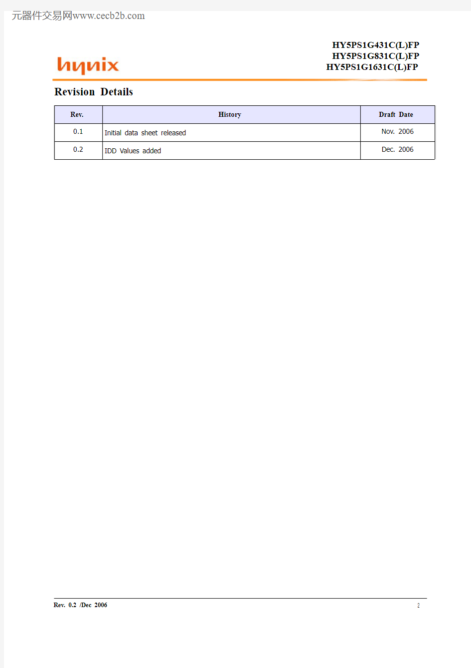
Revision Details
Rev.History
Draft Date 0.1Initial data sheet released Nov. 20060.2
IDD Values added
Dec. 2006
Rev. 0.2 / Dec 2006
3
Contents
1. Description
1.1 Device Features and Ordering Information
1.1.1 Key Φεατυρεσ1.1.2 Ordering Information 1.1.3 Ordering Frequency 1.2 Pin configuration 1.3 Pin Description
2. Maximum DC ratings
2.1 Absolute Maximum DC Ratings 2.2 Operating Temperature Condition
3. AC & DC Operating Conditions
3.1 DC Operating Conditions
5.1.1 Recommended DC Operating Conditions(SSTL_1.8)5.1.2 ODT DC Electrical Characteristics 3.2 DC & AC Logic Input Levels
3.2.1 Input DC Logic Level 3.2.2 Input AC Logic Level 3.2.3 AC Input Test Conditions 3.2.4 Differential Input AC Logic Level 3.2.5 Differential AC output parameters 3.3 Output Buffer Levels
3.3.1 Output AC Test Conditions 3.3.2 Output DC Current Drive 3.3.3 OCD default χηαραχτεριστιχσ
3.4 IDD Specifications & Measurement Conditions 3.5 Input/Output Capacitance
4. AC Timing Specifications
5. Package Dimensions
Rev. 0.2 /Dec 2006
4
1.1 Device Features & Ordering Information
1.1.1 Key Features
?VDD = 1.8V +/- 0.1V ?VDDQ = 1.8V +/- 0.1V
?All inputs and outputs are compatible with SSTL_18 interface ?8 banks
?Fully differential clock inputs (CK, /CK) operation ?Double data rate interface
?Source synchronous-data transaction aligned to bidirectional data strobe (DQS, DQS)?Differential Data Strobe (DQS, DQS)
?Data outputs on DQS, DQS edges when read (edged DQ)?Data inputs on DQS centers when write(centered DQ)
?On chip DLL align DQ, DQS and DQS transition with CK transition
?DM mask write data-in at the both rising and falling edges of the data strobe
?All addresses and control inputs except data, data strobes and data masks latched on the rising edges of the clock ?Programmable CAS latency 3, 4, 5 and 6 supported
?Programmable additive latency 0, 1, 2, 3, 4 and 5 supported
?Programmable burst length 4/8 with both nibble sequential and interleave mode ?Internal eight bank operations with single pulsed RAS ?Auto refresh and self refresh supported ?tRAS lockout supported ?8K refresh cycles /64ms
?JEDEC standard 60ball FBGA(x4/x8) , 84ball FBGA(x16)?Full strength driver option controlled by EMRS ?On Die Termination supported
?Off Chip Driver Impedance Adjustment supported ?Read Data Strobe supported (x8 only)?
Self-Refresh High Temperature Entry
Ordering Information
Part No.
Configuration Package
HY5PS1G431C(L)FP-XX*256Mx460 Ball
HY5PS1G831C(L)FP-XX*128Mx8HY5PS1G1631C(L)FP-XX*64Mx16
84 Ball Operating Frequency
Grade tCK(ns)
CL tRCD tRP Unit E35333Clk C4 3.75444Clk Y53555Clk S5
2.5
5
5
5
Clk
Note:
-XX* is the speed bin, refer to the Operation Frequency table for complete Part No.
1. Description
Rev. 0.2 /Dec 2006
5
1.2 Pin Configuration & Address Table
256Mx4 DDR2 Pin Configuration (Top view: see balls through package)
ROW AND COLUMN ADDRESS TABLE
ITEMS 256Mx4
# of Bank 8Bank Address BA0,BA1,BA2Auto Precharge Flag
A10/AP Row Address A0 - A13Column Address
A0-A9, A11Page size
1 KB
VSS DM VDDQ DQ3VSS WE BA1A1A5A9NC
NC VSSQ DQ1VSSQ VREF CKE
BA0A10
A3A7
A12
VDD NC VDDQ NC VDDL
BA2VSS VDD A B C D E F G H J K VSSQ DQS VDDQ DQ2VSSDL RAS CAS A2A6A11NC
DQS VSSQ DQ0VSSQ CK CK CS A0A4A8A13
VDDQ NC VDDQ NC VDD ODT
VDD
VSS
L
3
2
1
7
8
9
Rev. 0.2 /Dec 2006
6
128Mx8 DDR2 PIN CONFIGURATION (Top view: see balls through package)
ROW AND COLUMN ADDRESS TABLE
ITEMS 128Mx8
# of Bank 8Bank Address BA0, BA1, BA2
Auto Precharge Flag
A10/AP Row Address A0 - A13Column Address
A0-A9Page size
1 KB
VSS DM/RDQS VDDQ DQ3VSS WE BA1A1A5A9NC
NU/RDQS VSSQ DQ1VSSQ VREF CKE
BA0A10
A3A7
A12
VDD DQ6VDDQ DQ4VDDL
BA2VSS VDD A B C D E F G H J K VSSQ DQS VDDQ DQ2VSSDL RAS CAS A2A6A11NC
DQS VSSQ DQ0VSSQ CK CK CS A0A4A8A13
VDDQ DQ7VDDQ DQ5VDD ODT
VDD
VSS
L
3
2
1
7
8
9
Rev. 0.2 /Dec 2006
7
64Mx16 DDR2 PIN CONFIGURATION (Top view: see balls through package)
ROW AND COLUMN ADDRESS TABLE
ITEMS 64Mx16
# of Bank 8Bank Address BA0, BA1, BA2
Auto Precharge Flag
A10/AP Row Address A0 - A12Column Address
A0-A9Page size
2 KB
3
VSS UDM VDDQ DQ11VSS WE BA1A1A5A9NC, A14
2
NC VSSQ DQ9VSSQ VREF CKE
BA0A10/AP
A3A7
A12
1
VDD DQ14VDDQ DQ12VDDL
NC, BA2VSS VDD A F G H J K L M 7
VSSQ UDQS VDDQ DQ10VSSDL RAS CAS A2A6A11NC, A15
8
UDQS VSSQ DQ8VSSQ CK CK CS A0A4A8NC, A13
9
VDDQ DQ15VDDQ DQ13VDD ODT
VDD
VSS
VSS LDM VDDQ DQ3NC VSSQ DQ1VSSQ VDD DQ6VDDQ DQ4B C D E VSSQ LDQS VDDQ DQ2LDQS VSSQ DQ0VSSQ VDDQ DQ7VDDQ DQ5N P R
Rev. 0.2 /Dec 2006
8
IDD Test Conditions
(IDD values are for full operating range of Voltage and Temperature, Notes 1-5)
Symbol
Conditions
Units IDD0
Operating one bank active-precharge current ; t CK = t CK(IDD), t RC = t RC(IDD), t RAS = t RAS min(IDD) ; CKE is HIGH, CS is HIGH between valid commands;Address bus inputs are SWITCHING;Data bus inputs are SWITCHING
mA
IDD1
Operating one bank active-read-precharge current ; IOUT = 0mA;BL = 4, CL = CL(IDD), AL = 0; t CK = t CK(IDD), t RC = t RC (IDD), t RAS = t RASmin(IDD), t RCD = t RCD(IDD) ; CKE is HIGH, CS is HIGH between valid commands ; Address bus inputs are SWITCHING ; Data pattern is same as IDD4W
mA
IDD2P Precharge power-down current ; All banks idle ; t CK = t CK(IDD) ; CKE is LOW ; Other control and address bus inputs are STABLE; Data bus inputs are FLOATING
mA
IDD2Q Precharge quiet standby current ;All banks idle; t CK = t CK(IDD);CKE is HIGH, CS is HIGH; Other control and address bus inputs are STABLE; Data bus inputs are FLOATING
mA
IDD2N Precharge standby current ; All banks idle; t CK = t CK(IDD); CKE is HIGH, CS is HIGH; Other control and address bus inputs are SWITCHING; Data bus inputs are SWITCHING
mA IDD3P
Active power-down current ; All banks open; t CK = t CK(IDD); CKE is LOW; Other control and address bus inputs are STABLE; Data bus inputs are FLOATING Fast PDN Exit MRS(12) = 0mA Slow PDN Exit MRS(12) = 1mA
IDD3N Active standby current ; All banks open; t CK = t CK(IDD), t RAS = t RASmax(IDD), t RP
=t RP(IDD); CKE is HIGH, CS is HIGH between valid commands; Other control and address bus inputs are SWITCHING; Data bus inputs are SWITCHING
mA
IDD4W Operating burst write current ; All banks open, Continuous burst writes; BL = 4, CL = CL(IDD), AL = 0; t CK = t CK(IDD), t RAS = t RASmax(IDD), t RP = t RP(IDD); CKE is HIGH, CS is HIGH
between valid commands; Address bus inputs are SWITCHING; Data bus inputs are SWITCHING mA
IDD4R Operating burst read current ; All banks open, Continuous burst reads, IOUT = 0mA; BL = 4, CL = CL(IDD), AL = 0; t CK = t CK(IDD), t RAS = t RASmax(IDD), t RP = t RP(IDD); CKE is HIGH, CS is HIGH between valid commands; Address bus inputs are SWITCHING;; Data pattern is same as IDD4W
mA
IDD5B
Burst refresh current ; t CK = t CK(IDD); Refresh command at every t RFC(IDD) interval; CKE is HIGH, CS is HIGH between valid commands; Other control and address bus inputs are SWITCH-ING; Data bus inputs are SWITCHING
mA
IDD6
Self refresh current ; CK and CK at 0V; CKE £ 0.2V; Other control and address bus inputs are FLOATING; Data bus inputs are FLOATING
mA
IDD7Operating bank interleave read current ; All bank interleaving reads, IOUT = 0mA; BL = 4, CL = CL(IDD), AL = t RCD(IDD)-1*t CK(IDD); t CK = t CK(IDD), t RC = t RC(IDD), t RRD = t RRD(IDD), t RCD = 1*t CK(IDD); CKE is HIGH, CS is HIGH between valid commands; Address bus inputs are STABLE during DESELECTs; Data pattern is same as IDD4R; - Refer to the following page for detailed timing conditions
mA
Rev. 0.2 /Dec 2006
9
Note:
1.VDDQ = 1.8 +/- 0.1V ; VDD = 1.8 +/- 0.1V (exclusively VDDQ = 1.9 +/- 0.1V ; VDD = 1.9 +/- 0.1V for C3 speed grade)
2.IDD specifications are tested after the device is properly initialized
3.Input slew rate is specified by AC Parametric Test Condition
4.IDD parameters are specified with ODT disabled.
5.
Data bus consists of DQ, DM, DQS, DQS, RDQS, RDQS, LDQS, LDQS, UDQS, and UDQS. IDD values must be met with all combinations of EMRS bits 10 and 11.6.Definitions for IDD
LOW is defined as Vin £ VILAC(max)HIGH is defined as Vin ? VIHAC(min)
STABLE is defined as inputs stable at a HIGH or LOW level FLOATING is defined as inputs at VREF = VDDQ/2
SWITCHING is defined as: inputs changing between HIGH and LOW every other clock cycle (once per two clocks)for address and control signals, and inputs changing between HIGH and LOW every other data transfer (once per clock)for DQ signals not including masks or strobes.
Rev. 0.2 /Dec 2006
10
2. Maximum DC Ratings
2.1 Absolute Maximum DC Ratings
Note:
1.Stresses greater than those listed under “Absolute Maximum Ratings” may cause permanent damage to the device. This is a stress rating only and functional operation of the device at these or any other conditions above those indicated in the operational sections of this specification is not implied. Exposure to absolute maximum rat-ing conditions for extended periods may affect reliability.
2.Storage Temperature is the case surface temperature on the χεντερ/top side of the DRAM. For the measurement conditions. please refer to JESD51-2 standard.
2.2 Operating Temperature Condition
Note:
1.Operating Temperature is the case surface temperature on the center/top side of the DRAM. For the measure-ment conditions, please refer to JESD51-2 standard.
2.At 85~95° T OPER , Double refresh rate(tREFI:
3.9us) is required, and to enter the self refresh mode at this tem-perature range, an EMRS command is required to change ιnternal refresh rate.
Symbol Parameter
Rating Units Notes VDD Voltage on VDD pin relative to Vss - 1.0 V ~ 2.3 V V 1VDDQ Voltage on VDDQ pin relative to Vss - 0.5 V ~ 2.3 V V 1VDDL
Voltage on VDDL pin relative to Vss
- 0.5 V ~ 2.3 V V 1V IN, V OUT Voltage on any pin relative to Vss - 0.5 V ~ 2.3 V V
1
T STG Storage Temperature
-55 to +100°C 1, 2 I I Input leakage current; any input 0V VIN VDD; all other balls not under test = 0V)
-2 uA ~ 2 uA uA I OZ
Output leakage current; 0V VOUT VDDQ; DQ and ODT disabled
-5 uA ~ 5 uA
uA
Symbol Parameter Rating Units
Notes
T OPER Operating Temperature
0 to 95
°C 1,2
Rev. 0.2 /Dec 2006
11
3. AC & DC Operating Conditions
3.1 DC Operating Conditions
3.1.1 Recommended DC Operating Conditions (SSTL_1.8)
Note:
1.Min. Typ. and Max. values increase by 100mV for C3(DDR2-533 3-3-3) speed option.
2.VDDQ tracks with VDD,VDDL tracks with VDD. AC parameters are measured with VDD,VDDQ and VDD.
3.The value of VREF may be selected by the user to provide optimum noise margin in the system. Typically the value of VREF is expected to be about 0.5 x VDDQ of the transmitting device and VREF is expected to track varia-tions in VDDQ
4.Peak to peak ac noise on VREF may not exceed +/-2% VREF (dc).
5.VTT of transmitting device must track VREF of receiving device.
3.1.2 ODT DC electrical characteristics
Note :
1.Test condition for Rtt measurements
Measurement Definition for Rtt(eff):Apply V IH (ac) and V IL (ac) to test pin separately, then measure current I(V IH (ac)) and I(V IL (ac)) respectively. V IH (ac), V IL (ac), and VDDQ values defined in SSTL_18
Measurement Definition for VM :Measurement Voltage at test pin(mid point) with no load.
Symbol Parameter
Rating
Units Notes Min.Typ. Max.VDD Supply Voltage 1.7 1.8 1.9V 1VDDL Supply Voltage for DLL 1.7 1.8 1.9V 1,2VDDQ Supply Voltage for Output 1.7 1.8 1.9V 1,2VREF Input Reference Voltage 0.49*VDDQ 0.50*VDDQ 0.51*VDDQ mV 3,4VTT Termination Voltage
VREF-0.04
VREF
VREF+0.04
V
5
PARAMETER/CONDITION
SYMBOL MIN NOM MAX UNITS NOTES Rtt effective impedance value for EMRS(A6,A2)=0,1; 75 ohm Rtt1(eff)607590ohm 1Rtt effective impedance value for EMRS(A6,A2)=1,0; 150 ohm Rtt2(eff)120150180ohm 1Rtt effective impedance value for EMRS(A6,A2)=1,1; 50 ohm Rtt3(eff)4050
60ohm 1Deviation of VM with respect to VDDQ/2
delta VM
-6
+6
%
1
Rtt(eff) =
V IH (ac) - V IL (ac)I(V IH (ac)) - I(V IL (ac))
delta VM =
2 x Vm
VDDQ
x 100%
- 1
Rev. 0.2 /Dec 2006
12
3.2 DC & AC Logic Input Levels
3.2.1 Input DC Logic Level
3.2.2 Input AC Logic Level
3.2.3 AC Input Test Conditions
Note:
1.Input waveform timing is referenced to the input signal crossing through the V REF level applied to the device under test.
2.The input signal minimum slew rate is to be maintained over the range from V REF to V IH(ac) min for rising edges and the range from V REF to V IL(ac) max for falling edges as shown in the figure below.
3.AC timings are referenced with input waveforms switching from VIL(ac) to VIH(ac) on the positive transitions and VIH(ac) to VIL(ac) on the negative transitions.
Symbol Parameter Min.Max.Units Notes
V IH (dc)dc input logic high VREF + 0.125
VDDQ + 0.3V V IL (dc)
dc input logic low
- 0.3
VREF - 0.125
V
Symbol Parameter
DDR2 400,533DDR2 667,800Units Notes
Min.Max.Min.Max.V IH (ac)ac input logic high VREF + 0.250-VREF + 0.200
-V V IL (ac)
ac input logic low
-VREF - 0.250
-VREF - 0.200
V
Symbol Condition Value Units Notes V REF Input reference voltage
0.5 * V DDQ
V 1V SWING(MAX)
Input signal maximum peak to peak swing
1.0V 1SLEW Input signal minimum slew rate
1.0
V/ns
2, 3
Rev. 0.2 /Dec 2006
13
3.2.4 Differential Input AC logic Level
Note:
1.VIN(DC) specifies the allowable DC execution of each input of differential pair such as CK, CK, DQS, DQS, LDQS,LDQS, UDQS and UDQS.
2.VID(DC) specifies the input differential voltage |VTR -VCP | required for switching, where VTR is the true input (such as CK, DQS, LDQS or UDQS) level and VCP is the complementary input (such as CK, DQS, LDQS or UDQS) level.
The minimum value is equal to VIH(DC) - V IL(DC).
Note:
1.VID(AC) specifies the input differential voltage |VTR -VCP | required for switching, where VTR is the true input sig-nal
(such as CK, DQS, LDQS or UDQS) and VCP is the complementary input signal (such as CK, DQS, LDQS or UDQS). The minimum value is equal to V IH(AC) - V IL(AC).
2.The typical value of VIX(AC) is expected to be about 0.5 * VDDQ of the transmitting device and VIX(AC) is
expected to track variations in VDDQ. VIX(AC) indicates the voltage at which differential input signals must cross.
3.2.5 Differential AC output parameters
Note:
1.The typical value of VOX(AC) is expected to be about 0.5 * V DDQ of the transmitting device and VOX(AC) is expected to track variations in VDDQ. VOX(AC) indicates the voltage at ωηιχη differential output signals must cross.
Symbol Parameter
Min.Max.Units Notes V ID (ac)ac differential input voltage 0.5
VDDQ + 0.6V 1V IX (ac)ac differential cross point voltage
0.5 * VDDQ - 0.175
0.5 * VDDQ + 0.175
V
2
Symbol Parameter
Min.
Max.
Units Notes V OX (ac)ac differential cross point voltage
0.5 * VDDQ - 0.125
0.5 * VDDQ + 0.125
V
1
V DDQ
Crossing point
V SSQ
V TR V CP
V ID
V IX or V OX
< Differential signal levels >
Rev. 0.2 /Dec 2006
14
3.3 Output Buffer Characteristics
3.3.1 Output AC Test Conditions
Note:
1.The VDDQ of the device under test is referenced.
3.3.2 Output DC Current Drive
Note:
1.V DDQ = 1.7 V; V OUT = 1420 mV. (V OUT - V DDQ )/I OH must be less than 21 ohm for values of V OUT between V DDQ
and V DDQ - 280 mV.
2.V DDQ = 1.7 V; V OUT = 280 mV. V OUT /I OL must be less than 21 ohm for values of V OUT between 0 V and 280 mV.
3.The dc value of V REF applied to the receiving device is set to V TT
4.The values of I OH(dc) and I OL(dc) are based on the conditions given in Notes 1 and 2. They are used to test device drive current capability to ensure V IH min plus a noise margin and V IL max minus a noise margin are delivered to an SSTL_18 receiver. The actual current values are derived by shifting the desired driver operating point (see Section 3.3) along a 21 ohm load line to define a convenient driver current for measurement.
Symbol Parameter
SSTL_18 Class II
Units Notes V OTR Output Timing Measurement Reference Level
0.5 * V DDQ
V
1
Symbol Parameter
SSTl_18Units Notes I OH(dc)Output Minimum Source DC Current - 13.4mA 1, 3, 4I OL(dc)Output Minimum Sink DC Current
13.4
mA
2, 3, 4
Rev. 0.2 /Dec 2006
15
3.3.3 OCD default characteristics
Note :
1.Absolute Specifications ( Toper; VDD = +1.8V ±0.1V , VDDQ = +1.8V ±0.1V)
2.Impedance measurement condition for output source dc current: VDDQ=1.7V; VOUT=1420mV; (VOUT-VDDQ)/Ioh must be less than 2
3.4 ohms for values of VOUT between VDDQ and VDDQ-280mV
.
Impedance measurement condition for output sink dc current: VDDQ = 1.7V; VOUT = 280mV; VOUT/Iol must be less than 23.4 ohms for values of VOUT between 0V and 280mV .
3.Mismatch is absolute value between pull-up and pull-dn, both are measured at same temperature and voltage.
4.Slew rate measured from vil(ac) to vih(ac).
5.The absolute value of the slew rate as measured from DC to DC is equal to or greater than the slew rate as measured from AC to AC. This is guaranteed by design and characterization.
6.This represents the step size when the OCD is near 18 ohms at nominal conditions across all process
corners/variations and represents only the DRAM uncertainty. A 0 ohm value(no calibration) can only be achieved if the OCD impedance is 18 ohms +/- 0.75 ohms under nominal conditions.Output Slew rate load:
7.DRAM output slew rate specification applies to 400, 533 and 667 MT/s speed bins.
8.Timing skew due to DRAM output slew rate mis-match between DQS / DQS and associated DQs is included in tDQSQ and tQHS specification.
Description
Parameter Min Nom Max Unit Notes Output impedance
--
-ohms 1Output impedance step size for OCD calibration 0 1.5ohms 6Pull-up and pull-down mismatch 0
4
ohms 1,2,3Output slew rate Sout 1.5-5
V/ns
1,4,5,6,7,8
Rev. 0.2 /Dec 2006
16
IDD Specifications(max)
Symbol
DDR2 400DDR2 533
DDR2 667
DDR2 800
Units
x4
x8x4x8x16x4x8x16x4x8x16IDD06060656585707090757595mA IDD17070757511080801158585120mA IDD2P 88888888888mA IDD2Q 2222272727303030323232mA IDD2N 3030353535404040454545mA IDD3P
F 2020202020252525252525mA S
99999999999mA IDD3N 3535454545505050555555mA IDD4W 100100125125160150150195170170225mA IDD4R 100100125125160150150195170170225mA IDD5
165165165165165175175175175175175mA IDD6
Normal
88888888888mA Low power 55555555555mA IDD7
165
165
175
175
260
180
180
265
185
185
270
mA
3.4 IDD Specifications & Test Conditions
Rev. 0.2 /Dec 2006
17
IDD Test Conditions
(IDD values are for full operating range of Voltage and Temperature, Notes 1-5)
Symbol Conditions
Units IDD0
Operating one bank active-precharge current ; t CK = t CK(IDD), t RC = t RC(IDD), t RAS = t RAS min(IDD) ; CKE is HIGH, CS is HIGH between valid commands;Address bus inputs are SWITCH-ING;Data bus inputs are SWITCHING
mA
IDD1
Operating one bank active-read-precharge χυρρεντ ; IOUT = 0mA;BL = 4, CL = CL(IDD), AL = 0; t CK = t CK(IDD), t RC = t RC (IDD), t RAS = t RASmin(IDD), t RCD = t RCD(IDD) ; CKE is HIGH, CS is HIGH between valid commands ; Address bus inputs are SWITCHING ; Data pattern is same as IDD4W
mA
IDD2P Precharge power-down current ; All banks idle ; t CK = t CK(IDD) ; CKE is LOW ; Other control and address bus inputs are STABLE; Data bus inputs are FLOATING
mA IDD2Q Precharge quiet standby current ;All banks idle; t CK = t CK(IDD);CKE is HIGH, CS is HIGH; Other control and address bus inputs are STABLE; Data bus inputs are FLOATING
mA IDD2N
Precharge standby current ; All banks idle; t CK = t CK(IDD); CKE is HIGH, CS is HIGH; Other control and address bus inputs are SWITCHING; Data bus inputs are SWITCHING
mA IDD3P
Active power-down current ; All banks open; t CK = t CK(IDD); CKE is LOW; Other control and address bus inputs are STABLE; Data bus inputs are FLOATING Fast PDN Exit MRS(12) = 0mA Slow PDN Exit MRS(12) = 1mA
IDD3N Active standby current ; All banks open; t CK = t CK(IDD), t RAS = t RASmax(IDD), t RP
=t RP(IDD); CKE is HIGH, CS is HIGH between valid commands; Other control and address bus inputs are SWITCHING; Data bus inputs are SWITCHING
mA
IDD4W Operating burst write current ; All banks open, Continuous burst writes; BL = 4, CL = CL(IDD), AL = 0; t CK = t CK(IDD), t RAS = t RASmax(IDD), t RP = t RP(IDD); CKE is HIGH, CS is HIGH between valid commands; Address bus inputs are SWITCHING; Data bus inputs are SWITCHING
mA
IDD4R Operating burst read current ; All banks open, Continuous burst reads, IOUT = 0mA; BL = 4, CL = CL(IDD), AL = 0; t CK = t CK(IDD), t RAS = t RASmax(IDD), t RP = t RP(IDD); CKE is HIGH, CS is HIGH between valid commands; Address bus inputs are SWITCHING;; Data pattern is same as IDD4W
mA
IDD5B
Burst refresh current ; t CK = t CK(IDD); Refresh command at every t RFC(IDD) interval; CKE is HIGH, CS is HIGH between valid commands; Other control and address bus inputs are SWITCH-ING; Data bus inputs are SWITCHING
mA
IDD6
Self refresh current ; CK and CK at 0V; CKE £ 0.2V; Other control and address bus inputs are FLOATING; Data bus inputs are FLOATING
mA
FLOATING is defined as inputs at VREF = VDDQ/2
SWITCHING is defined as: inputs changing between HIGH and LOW every other clock cycle (once per two clocks) for address and control signals, and inputs changing between HIGH and LOW every other data transfer (once per clock) for DQ signals not including masks or strobes.
IDD7Operating bank interleave read current ; All bank interleaving reads, IOUT = 0mA; BL = 4, CL = CL(IDD), AL = t RCD(IDD)-1*t CK(IDD); t CK = t CK(IDD), t RC = t RC(IDD), t RRD = t RRD(IDD), t RCD = 1*t CK(IDD); CKE is HIGH, CS is HIGH between valid commands; Address bus inputs are STABLE during DESELECTs; Data pattern is same as IDD4R; - Refer to the following page for detailed timing conditions
mA
Rev. 0.2 /Dec 2006
18
Note :
1.VDDQ = 1.8 +/- 0.1V ; VDD = 1.8 +/- 0.1V (exclusively VDDQ = 1.9 +/- 0.1V ; VDD = 1.9 +/- 0.1V for C3 speed grade)
2.IDD specifications are tested after the device is properly initialized
3.Input slew rate is specified by AC Parametric Test Condition
4.IDD parameters are specified with ODT disabled.
5.Data bus consists of DQ, DM, DQS, DQS, RDQS, RDQS, LDQS, LDQS, UDQS, and UDQS. IDD values must be met with all combinations of EMRS bits 10 and 11.
6.Definitions for IDD
LOW is defined as Vin £ VILAC(max)HIGH is defined as Vin ? VIHAC(min)
STABLE is defined as inputs stable at a HIGH or LOW level FLOATING is defined as inputs at VREF = VDDQ/2
SWITCHING is defined as: inputs changing between HIGH and LOW every other clock cycle (once per two clocks)for address and control signals, and inputs changing between HIGH and LOW every other data transfer (once per clock) for DQ signals not including masks or strobes.
Rev. 0.2 /Dec 2006
19
For purposes of IDD testing, the following parameters are to be utilized
Detailed IDD7
The detailed timings are shown below for IDD7. Changes will be required if timing parameter changes are made to the specification.
Legend: A = Active; RA = Read with Autoprecharge; D = Deselect
IDD7: Operating Current: All Bank Interleave Read operation
All banks are being interleaved at minimum t RC(IDD) without violating t RRD(IDD) using a burst length of 4. Control and address bus inputs are STABLE during DESELECTs. IOUT = 0mA Timing Patterns for 4 bank devices x4/ x8/ x16
-DDR2-400 4/4/4: A0 RA0 A1 RA1 A2 RA2 A3 RA3 D D D D D -DDR2-400 3/3/3: A0 RA0 A1 RA1 A2 RA2 A3 RA3 D D D D
-DDR2-533 5/4/4: A0 RA0 D A1 RA1 D A2 RA2 D A3 RA3 D D D D D -DDR2-533 4/4/4: A0 RA0 D A1 RA1 D A2 RA2 D A3 RA3 D D D D D
Timing Patterns for 8 bank devices x4/8
-DDR2-400 all bins: A0 RA0 A1 RA1 A2 RA2 A3 RA3 A4 RA4 A5 RA5 A6 RA6 A7 RA7-DDR2-533 all bins: A0 RA0 A1 RA1 A2 RA2 A3 RA3 D D A4 RA4 A5 RA5 A6 RA6 A7 RA7 D D Timing Patterns for 8 bank devices x16
-DDR2-400 all bins: A0 RA0 A1 RA1 A2 RA2 A3 RA3 D D A4 RA4 A5 RA5 A6 RA6 A7 RA7 D D
-DDR2-533 all bins: A0 RA0 D A1 RA1 D A2 RA2 D A3 RA3 D D D A4 RA4 D A5 D A6 RA6 D A7 RA7 D D D
DDR2-800
DDR2-667DDR2-533DDR2-400Parameter 5-5-56-6-65-5-54-4-43-3-3Units CL(IDD)56543tCK t RCD(IDD)12.515151515ns t RC(IDD)57.560606055ns t RRD(IDD)-x4/x87.57.57.57.57.5ns t RRD(IDD)-x161010101010ns t CK(IDD) 2.5 2.53 3.755ns t RASmin(IDD)4545454540ns t RASmax(IDD)7000070000700007000070000ns t RP(IDD)12.515151515ns t RFC(IDD)-256Mb 7575757575ns t RFC(IDD)-512Mb 105105105105105ns t RFC(IDD)-1Gb 127.5127.5127.5127.5127.5ns t RFC(IDD)-2Gb
197.5
197.5
197.5
197.5
197.5
ns
Rev. 0.2 /Dec 2006
20
3.5. Input/Output Capacitance
4. Electrical Characteristics & AC Timing Specification
( 0 ?? ?? T CASE ?? 95??; V DDQ = 1.8 V +/- 0.1V; V DD = 1.8V +/- 0.1V)
Refresh Parameters by Device Density
DDR2 SDRAM speed bins and tRCD, tRP and tRC for corresponding bin
Note 1: 8 bank device Precharge All Allowance : tRP for a Precharge All command for an 8 Bank device will equal to
tRP+1*tCK, where tRP are the values for a single bank Πρεχηαργε, which are shown in the table above.
Parameter Symbol DDR2 400DDR2 533DDR2 667DDR2 800Units
Min
Max Min Max Input capacitance, CK and CK CCK 1.0 2.0 1.0 2.0pF Input capacitance delta, CK and CK CDCK x 0.25x 0.25pF Input capacitance, all other input-only pins CI 1.0 2.0 1.0 2.0pF Input capacitance delta, all other input-only pins CDI x 0.25x 0.25pF Input/output capacitance, DQ, DM, DQS, DQS CIO 2.5 4.0 2.5 3.5pF Input/output capacitance delta, DQ, DM, DQS, DQS
CDIO
x
0.5
x
0.5
pF
Parameter
Symbol 256Mb 512Mb 1Gb 2Gb 4Gb Units Refresh to Active/Refresh command
time tRFC
75105127.5195327.5ns Average periodic refresh interval
tREFI
0 ????T CASE ?? 95??7.87.87.87.87.8ns 85??≤…T CASE ?? 95??
3.9
3.9
3.9
3.9
3.9
ns
Speed DDR2-800DDR2-667DDR2-533DDR2-400Units
Bin(CL-tRCD-tRP)
5-5-56-6-64-4-45-5-54-4-43-3-3Parameter min min min min min min CAS Latency
564543tCK tRCD 12.51512151515ns tRP Note112.51512151515ns tRAS 454545454540ns tRC
57.5
60
57
60
60
55
ns