UDN2944中文资料
Capable of driving loads to 4 A at supply voltages to 60 V (induc-tive loads to 35 V), the UDN2944W is a quad high-current, high-voltage source driver. Each of the four power drivers can provide space- and cost-saving interface between low-level signal-processing circuits and high-power loads in harsh environments.
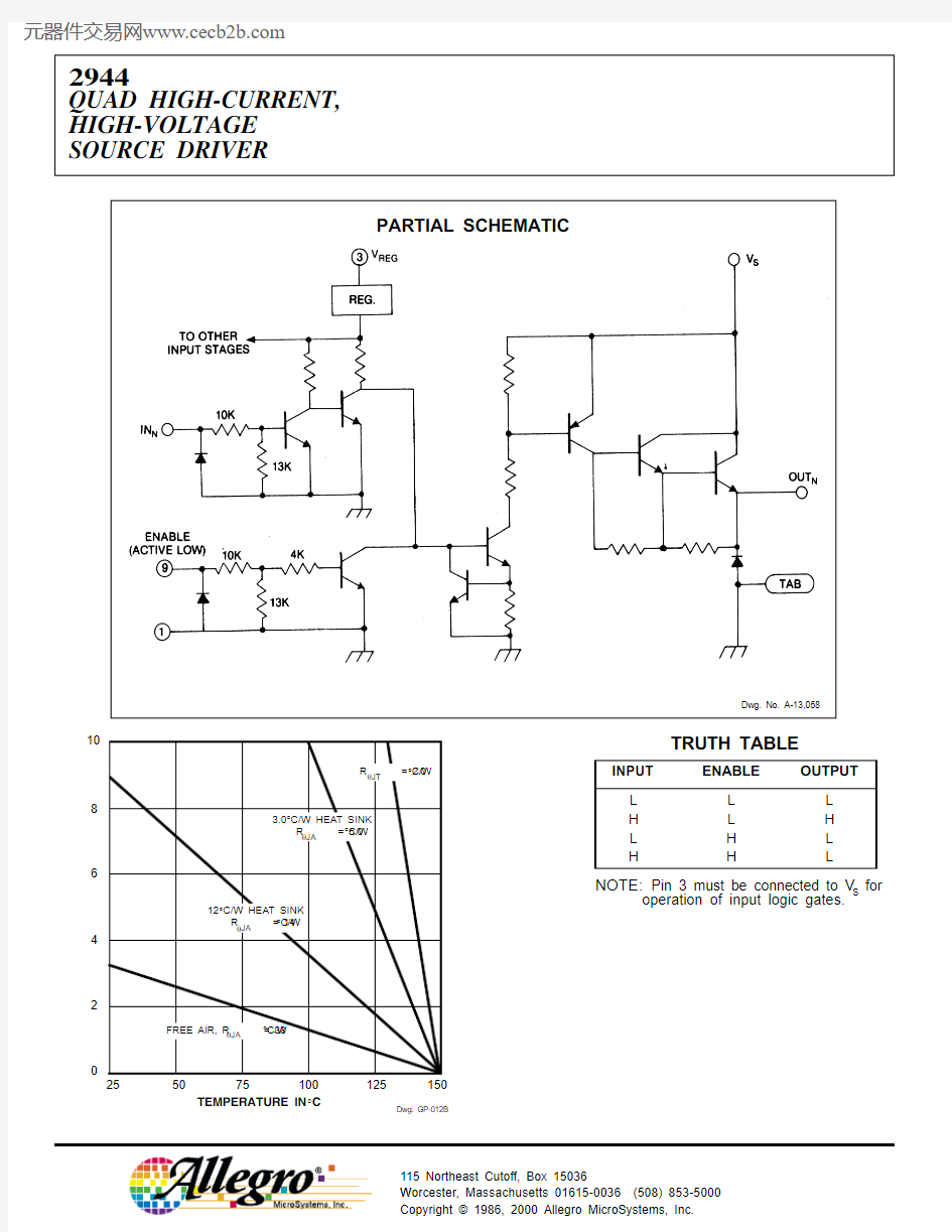
Individual supply lines have been provided for each pair of drivers so that different supplies can be used to drive multiple loads. The controlling inputs are TTL or CMOS compatible. The outputs include transient-suppression diodes for inductive loads.
This quad Darlington array is designed to serve as an interface between low-level circuitry and peripheral-power loads such as sole-noids, motors, incandescent displays, heaters, and similar loads of up to 240 W per channel. The UDN2944W is an ideal complement to the UDN2878W quad 4 A sink driver.
For maximum power-handling capability, the UDN2944W driver is supplied in a 12-pin single in-line, power-tab package that allows efficient attachment of an external heat sink for maximum allowable package power dissipation. An external heat sink is usually required for proper operation of this device. The tab is at ground potential and needs no insulation.
FEATURES
I Output Current to 4 A I Output Voltage to 60 V I Loads to 960 W
I Integral Output Suppression Diodes I TTL and CMOS Compatible Inputs I Plastic Single In-Line Package I
Heat-Sink Tab
2944
QUAD HIGH-CURRENT,
HIGH-VOLTAGE SOURCE DRIVER
ABSOLUTE MAXIMUM RATINGS at +25°C Free-Air Temperature
Supply Voltage Range, V S ..... 10 V to 60 V Output Current, I OUT
(continuous)............................... -4.0 A (peak)......................................... -5.0 A Input Voltage, V IN ................................ 15 V Package Power Dissipation,
P D ....................................... See Graph Operating Temperature Range,
T A ................................ -20°C to +85°C Storage Temperature Range,
T S .............................. -55°C to +150°C Output current rating will be limited by ambient temperature, duty cycle, heat sinking, air flow, and number of outputs
conducting. Under any set of conditions, do not exceed the -5.0 A peak current or a junction temperature of +150°C.
V S
Data Sheet 29309.10?
2944
QUAD HIGH-CURRENT,HIGH-VOLTAGE
SOURCE DRIVER
115 Northeast Cutoff, Box 15036Worcester, Massachusetts 01615-0036 (508) 853-5000
PARTIAL SCHEMATIC
50
75100
125
150
10
6
4
2
0A L L O W A B L E P A C K A G E P O W E R D I S S I P A T I O N I N W A T T S
TEMPERATURE IN °C
8
25
Dwg. GP-012B
W Copyright ? 1986, 2000 Allegro MicroSystems, Inc.
TRUTH TABLE
INPUT ENABLE
OUTPUT
L
L L H L H L H L H
H
L
NOTE:Pin 3 must be connected to V S for
operation of input logic gates.
Dwg. No. A-13,058
2944
QUAD HIGH-CURRENT,
HIGH-VOLTAGE SOURCE DRIVER
https://www.sodocs.net/doc/062442182.html,
ELECTRICAL CHARACTERISTICS at T A = +25°C, T J ≤ +150°C, V S = 60 V, V ENABLE = 0 V (unless otherwise noted).
Limits Characteristic Symbol Test Conditions
Min.Max.Units Supply Voltage Range V S 1060V Output Leakage Current I CEX V OUT = 0 V, V ENABLE = 2.4 V —50μA Output Sustaining Voltage V CE(sus)I OUT = -4 A, L = 3 mH 35—V Output Saturation Voltage
V CE(SAT)
I OUT = -1 A, V IN = 2.4 V — 1.8V I OUT = -4 A, V IN = 2.4 V
— 2.5V Input Voltage
Logic 1V IN(1) or V ENABLE(1) 2.0—V Logic 0
V IN(0) or V ENABLE(0)
—0.8V Input Current
Logic 1
V IN(1) or V ENABLE(1) = 2.4 V —220μA V IN(1) or V ENABLE(1) = 12 V
— 1.5mA Logic 0
V IN(0) or V ENABLE(0) = 0.8 V —50μA Total Supply Current
I S All drivers on, All outputs open —25mA Clamp Diode Leakage Current I R V R = 60 V —50μA Clamp Diode Forward Voltage V F I F = 4 A
— 2.2V Turn-On Delay t ON 0.5 E in to 0.5 E out , R L = 15 ?— 2.0μs Turn-Off Delay
t OFF
0.5 E in to 0.5 E out , R L = 15 ?—
10
μs
NOTE: Negative current is defined as coming out of (sourcing) the device being tested.
2944
QUAD HIGH-CURRENT,HIGH-VOLTAGE
SOURCE DRIVER
115 Northeast Cutoff, Box 15036
Worcester, Massachusetts 01615-0036 (508) 853-5000
Dimensions in Inches
(controlling dimensions)
NOTES:1.
Lead thickness is measured at seating plane or below.2.Lead spacing tolerance is non-cumulative.
3.Exact body and lead configuration at vendor’s option within limits shown.
4.Lead gauge plane is 0.030” below seating plane.
5.Supplied in standard sticks/tubes of 15 devices.
Dwg. MP-007 in
2944 QUAD HIGH-CURRENT,
HIGH-VOLTAGE
SOURCE DRIVER
https://www.sodocs.net/doc/062442182.html, Dimensions in Millimeters (for reference only)
NOTES:1.Lead thickness is measured at seating plane or below.
2.Lead spacing tolerance is non-cumulative.
3.Exact body and lead configuration at vendor’s option within limits shown.
4.Lead gauge plane is 0.762 mm below seating plane.
5.Supplied in standard sticks/tubes of 15 devices.Dwg. MP-007 mm
2944
QUAD HIGH-CURRENT,HIGH-VOLTAGE
SOURCE DRIVER
115 Northeast Cutoff, Box 15036
Worcester, Massachusetts 01615-0036 (508) 853-5000
This page intentionally left blank
2944 QUAD HIGH-CURRENT,
HIGH-VOLTAGE
SOURCE DRIVER
https://www.sodocs.net/doc/062442182.html,
The products described here are manufactured under one or more U.S. patents or U.S. patents pending.
Allegro MicroSystems, Inc. reserves the right to make, from time to time, such departures from the detail specifications as may be required to permit improvements in the performance, reliability, or manufacturability of its products. Before placing an order, the user is cautioned to verify that the information being relied upon is current.
Allegro products are not authorized for use as critical components in life-support devices or systems without express written approval.
The information included herein is believed to be accurate and reliable. However, Allegro MicroSystems, Inc. assumes no responsi-bility for its use; nor for any infringement of patents or other rights of third parties which may result from its use.
2944
QUAD HIGH-CURRENT,HIGH-VOLTAGE
SOURCE DRIVER
115 Northeast Cutoff, Box 15036
Worcester, Massachusetts 01615-0036 (508) 853-5000
POWER SOURCE DRIVERS
IN ORDER OF 1) OUTPUT CURRENT, 2) OUTPUT VOLTAGE, 3) NUMBER OF DRIVERS
Output Ratings *Features
Serial Latched Diode Saturated Internal
mA V #Input Drivers Clamp Outputs Protection Part Number
?
-2560 8–X –––581560
10
X
X active pull-down –
–5810-F and 6809/106012X X active pull-down ––5811 and 6811
6020X X active pull-down ––5812-F and 68126032X X active pull-down ––5818-F and 681885 8–––––6118
-120-25 8––X X –2585
30 8––X X –298550 8X X X X –589
5
-35035 8––X –X 2987
50 8––X ––2981 and 298250 8X X X ––5891-50 8––X ––258080 8––X ––2983 and 298480 8X X X ––5890-80 8––X ––2588
-50061–––MOSFET X 2525 and 2535
62–––MOSFET X 2526 and 2536
-4000604––X ––2944
over-current protection voltage limits.
?Complete part number includes additional characters to indicate operating temperature range and package style.